Touch control electrode layer and display panel

A touch electrode and display panel technology, applied in static indicators, electrical digital data processing, instruments, etc., can solve the problems of display function and touch function signal error, signal interference, etc., and achieve the effect of improving induction sensitivity

Active Publication Date: 2009-04-22
AU OPTRONICS CORP
View PDF0 Cites 20 Cited by
  • Summary
  • Abstract
  • Description
  • Claims
  • Application Information

AI Technical Summary

Problems solved by technology

In this way, the scanning signal of the touch function and the driving signal of the liquid crystal display panel will interfere with each other (coupling), which will lead to signal errors of the display function and the touch function.
In addition, when the capacitive touch electrodes are embedded in the position b, the liquid crystal display panel will generate larger parasitic capacitance due to the closer distance between the touch electrodes and the electrode film 105 , thus causing more serious signal interference.

Method used


Image

  • Touch control electrode layer and display panel
  • Touch control electrode layer and display panel
  • Touch control electrode layer and display panel

Examples


no. 1 example

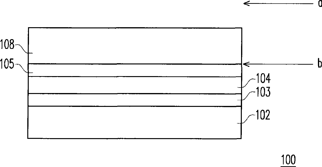
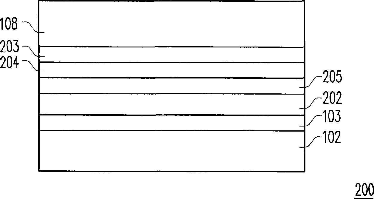
[0068] figure 2 is a schematic cross-sectional view of the display panel according to the first embodiment of the present invention. Please refer to figure 2 , the display panel 200 of this embodiment includes a first substrate 102 , a pixel array 103 , a second substrate 108 , a display medium 202 and a touch electrode layer 203 .

[0069] The first substrate 102 and the second substrate 108 can be made of glass, plastic, silicon, metal or other suitable substrate materials. The second substrate 108 is located opposite to the first substrate 102 .

[0070] The pixel array 103 is located on the first substrate 102 . The pixel array 103 is composed of several pixel structures, including multiple active components, multiple scan lines, multiple data lines, and multiple pixel electrodes (not shown). The active component is electrically connected to the scan line and the data line, and the pixel electrode is electrically connected to the corresponding active component. The ...

no. 2 example

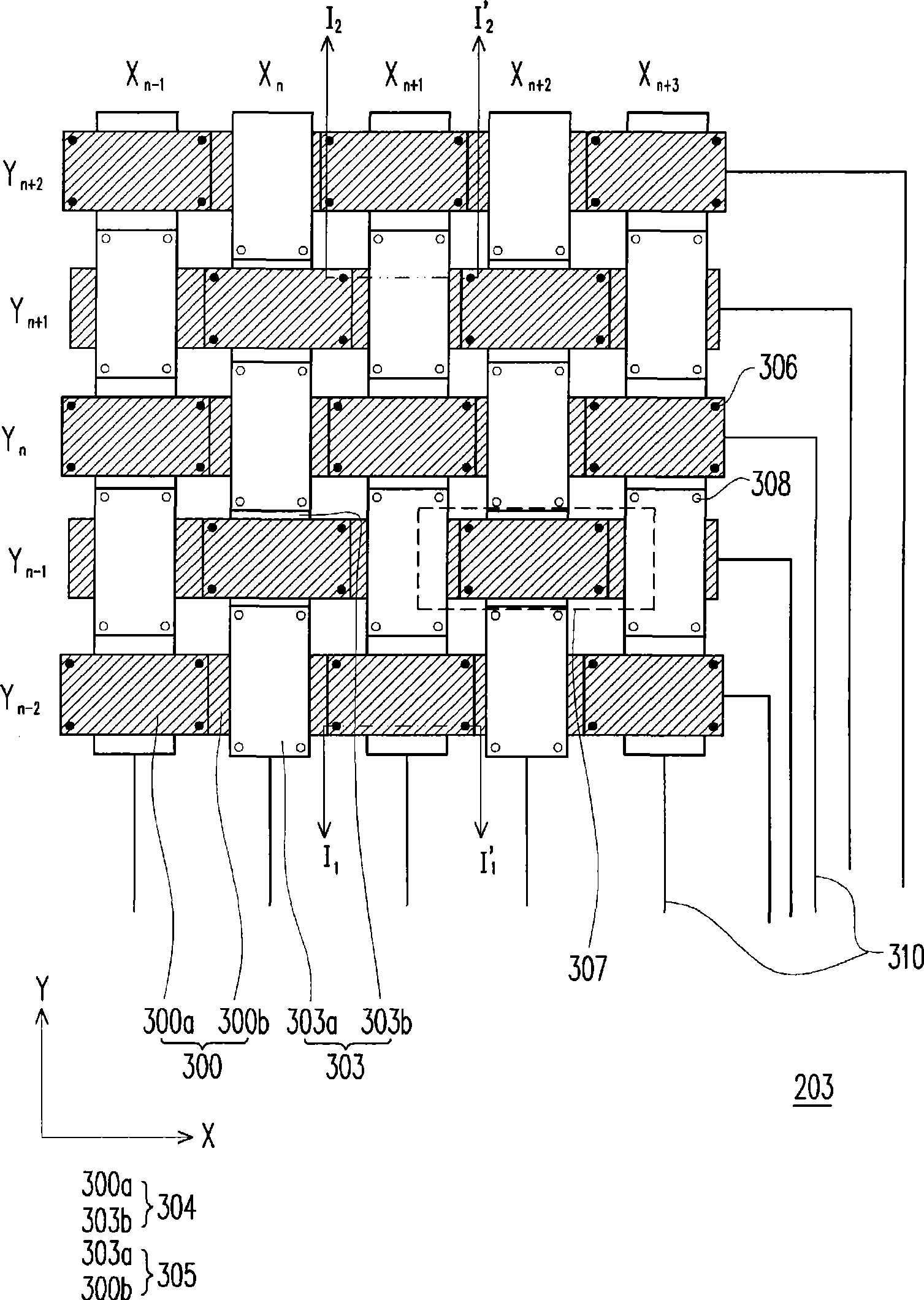
[0082] FIG. 7 is a schematic top view of a touch electrode layer according to a second embodiment of the present invention. Please refer to Figure 7, this embodiment and image 3 The touch electrode layer 203 of the embodiment is similar, except that the touch electrode layer 700 of this embodiment is divided into at least two regions. In FIG. 7 , the touch electrode layer 700 is divided into four regions A, B, C, and D, but the number of regions is not limited in the present invention.

[0083] In FIG. 7 , the first touch electrode 706 and the second touch electrode 708 in area A are different from the first touch electrodes 702, 716, 718 and second touch electrodes in the other three areas B, C, and D. 704, 720, 722 insulation. Moreover, each of the first touch electrodes 706 and each of the second touch electrodes 708 in the area A is electrically connected to a peripheral circuit 712 respectively. Similarly, the first touch electrodes 702 and the second touch electrodes...


PUM

PropertyMeasurementUnit
Thicknessaaaaaaaaaa

Abstract

A display panel comprises a first substrate, a second substrate and a display media; wherein, the display media is positioned between the first substrate and second substrate. The first substrate is provided with a pixel array. The second substrate includes a plurality of first contact control electrodes arranged along a first direction and a plurality of second contact control electrodes arranged along a second direction. Each of the first contact control electrodes is formed by staggered arranging a plurality of first upper layer contact control electrode patterns and a plurality of first lower layer shield electrode patterns, and each of the first upper layer contact control electrode patterns is electrically connected with the coadjacent first upper layer contact control electrode pattern. Each of the second contact control electrodes is formed by staggered arranging a plurality of second upper layer contact control electrode patterns and a plurality of second lower layer shield electrode patterns, and each of the second upper layer contact control electrode patterns is electrically connected with the coadjacent second upper layer contact control electrode pattern.

Description

【Technical field】 [0001] The present invention relates to a touch electrode layer and a display panel, and in particular to a touch electrode layer capable of reducing the parasitic capacitance between the touch electrode layer and the electrode layer in the display panel, and a touch electrode layer with the touch control electrode layer. The electrode layer of the display panel. 【Background technique】 [0002] Generally, existing touch display panels can be roughly classified into capacitive, resistive, and photosensitive types based on the design principle of the touch function. According to the structural classification of the touch function, it can be divided into two types: external sticker type and built-in type. Capacitive touch display panels have become a mainstream new development trend in the market due to their higher aperture ratio and better signal-to-noise ratio. The thickness of the in-cell touch display panel is thinner than that of the external touch dis...

Claims


Application Information

Patent Timeline
IPC IPC(8): G02F1/133G06F3/044
Inventor 李明宪周诗博杨敦钧李锡烈
Owner AU OPTRONICS CORP
Why Eureka
Try Eureka