Method for detecting equipment parameter filtrating chip conical defect through regulating detect

A technology for equipment parameter and defect inspection, which is applied in the direction of optical test defect/defect, semiconductor/solid-state device test/measurement, etc., can solve problems such as difficult-to-filter cone-shaped defects, affect the accuracy of scanning detection effect, etc., and achieve improved scanning effect Effect

Inactive Publication Date: 2009-04-22
SEMICON MFG INT (SHANGHAI) CORP +1
View PDF0 Cites 7 Cited by
  • Summary
  • Abstract
  • Description
  • Claims
  • Application Information

AI Technical Summary

Problems solved by technology

[0006] 2. In the process of scanning with equipment, since the scattering intensity of cone-shaped defects is very high, and the scanning equipment detects defects according to the intensity of scattering, these cone-shaped defects can be easily detected
Howe

Method used


Image

  • Method for detecting equipment parameter filtrating chip conical defect through regulating detect
  • Method for detecting equipment parameter filtrating chip conical defect through regulating detect
  • Method for detecting equipment parameter filtrating chip conical defect through regulating detect

Examples


Embodiment Construction

[0040] Describe in detail below in conjunction with accompanying drawing.

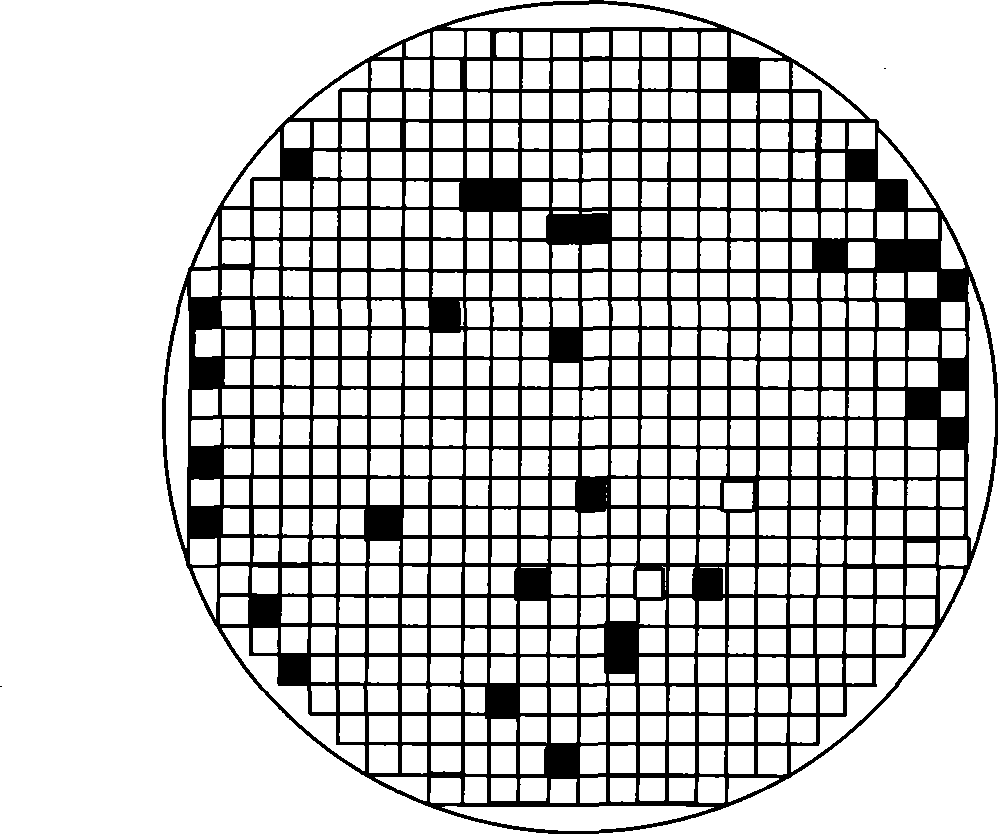
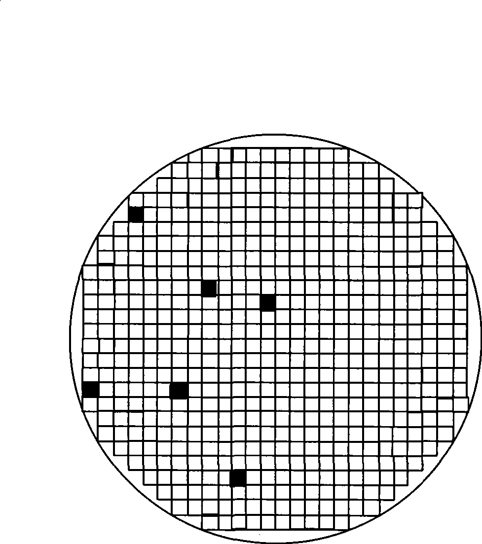
[0041] The scanning device used in this article is a defect inspection device named AIT (advanced inspection technoLogy) produced by KLA-Tencor.

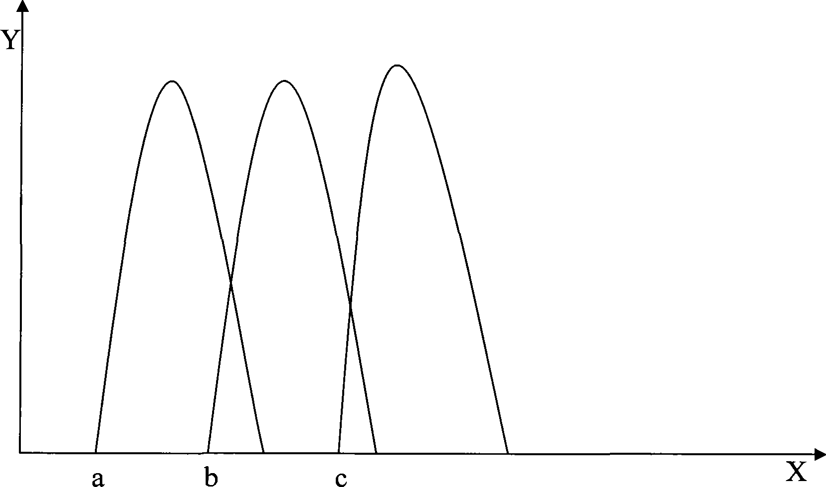
[0042] A method for filtering chip cone-shaped defects by adjusting defect inspection equipment parameters, the three parameters of Lo are the voltage values ​​of three dynamic scattering receivers, comprising the following steps:

[0043] A, Adjust the three values ​​of the scanning device machine system parameter Lo between the system default value and 0 for a given polarization combination.

[0044] Lo is one of the system parameters of the scanning device, which has three values, and the wind corresponds to the three dynamic scattering receivers of the scanning device. These three values ​​are used to adjust the voltages of the three receiving devices, which determine the intensity of the received laser light scattering. Low voltage values ​​make these...


PUM


Abstract

The invention relates to a method for filtering the conical defects of a chip by regulating the parameters of a defect inspection device, and the method comprises the following steps: step A, three values of the system parameters Lo of a scanning device machine are adjusted to be between the system default values and 0 under the situation of the given polarization combination; step B, different regions are selected under the full chip observation mode of the scanning device machine, the region in the mapping function is selected as a logic region, then the histogram function is selected to obtain a distribution diagram of scattering dynamic received intensities of three receivers in the region; step C, three values of the transverse coordinates of the corresponding points which start to increase at the left sides of three peak forms on the distribution diagram are determined on the distribution diagram of the scattering dynamic received intensities of the three receivers in the region, that is the three values of the Lo parameters; step D, the three Lo parameters obtained in the step C are used as the Lo parameter values for carrying out the scanning. The method can not only ensure the conical defects of the open region to be successfully filtered, but also ensure the killer defects of the logic region not to be missed by the inspection.

Description

technical field [0001] The invention relates to a method for filtering chip cone-shaped defects by adjusting parameters of defect inspection equipment in the field of semiconductor chip manufacturing. Background technique [0002] In the field of semiconductor chip production, it is necessary to scan and inspect the surface of each wafer chip to find defects on the chip surface, separate normal chips from abnormal and defective chips, and eventually abnormal chips will be rejected, and normal chips will continue into the process. There are many inspection tools for this type of defect detection. The principle is to use a laser to scan the surface of the chip, judge whether there is a defect on the chip according to the intensity of the received scattered signal, and identify the defective chip. [0003] There are many types of chip defects, some of which are called killer defects. The presence of such defects will change the electrical properties of the chip. For example...

Claims


Application Information

Patent Timeline
IPC IPC(8): H01L21/66G01N21/93G01N21/95
Inventor 马利华张书玉
Owner SEMICON MFG INT (SHANGHAI) CORP
Why Eureka
Try Eureka