Method for manufacturing flexible printed circuit board and detection method thereof

A flexible printing and inspection method technology, applied in the directions of printed circuit manufacturing, printed circuits, circuit inspection/monitoring/correction, etc., can solve the problems of not being able to obtain stable inspection quality, reducing the reliability of electrical inspection, increasing production costs, etc. Check performance, improve competitiveness, reduce the effect of manufacturing process

Inactive Publication Date: 2009-04-29
AJUHITEK
View PDF0 Cites 8 Cited by
  • Summary
  • Abstract
  • Description
  • Claims
  • Application Information

AI Technical Summary

Problems solved by technology

[0007] As mentioned above, recently, since a very fine circuit pattern is formed on a flexible printed circuit board for a driver integrated circuit of a display device, there are very fine defective products whose circuit pattern's open circuit / short width is, for example, about 2 μm or less, and the electrical inspection is reliable. decreased sex
In particular, the open circuit / short circuit width of the circuit pattern is very small. In the existing electrical inspection process of open circuit / short circuit, it is an over-inspection phenomenon that the actual qualified product is judged as a defective product or the actual defective product is judged as a non-conforming product. The non-detection phenomenon of qualified products increases geometrically, resulting in increased production costs, and cannot obtain stable inspection quality
Therefore, it has become the main reason for the reduction of the competitiveness of manufacturing companies.

Method used


Image

  • Method for manufacturing flexible printed circuit board and detection method thereof
  • Method for manufacturing flexible printed circuit board and detection method thereof
  • Method for manufacturing flexible printed circuit board and detection method thereof

Examples


Embodiment Construction

[0042] Various modifications are possible for the embodiments of the present invention, and the scope of the present invention is not limited to the embodiments described below. The embodiments of the present invention are intended to provide more sufficient explanations to those skilled in the art. Therefore, the shapes and the like of the components in the drawings are exaggerated for further emphasis.

[0043] Refer below Figure 1 ~ Figure 1 0 The embodiments of the present invention will be described in detail.

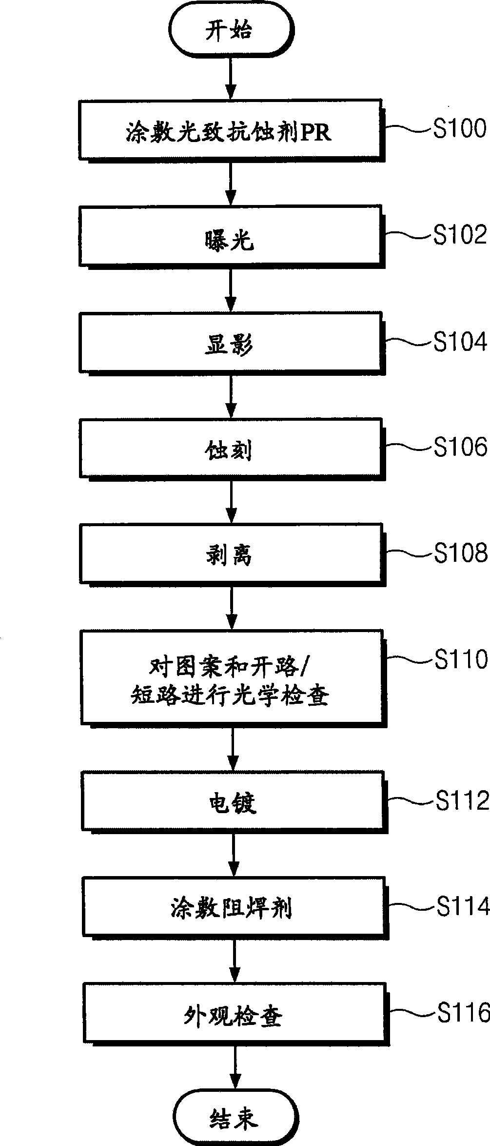
[0044] figure 1It is a flowchart showing the manufacturing procedure of the flexible printed circuit board for a display driver chip having an ultrafine circuit pattern of the present invention.

[0045] Such as figure 1 As shown, the manufacturing sequence of the flexible printed circuit board of the present invention is as follows: in step S100, a photoresist is coated on the base plate provided with copper foil, and in step S102 and step S104, exposure and...


PUM


Abstract

The invention provides a manufacture method of flexible printed circuit boards and inspection method thereof. In the manufacture method of the invention, whether a circuit pattern is qualified is detected and open-circuit and short-circuit unqualified products are detected by an optical check process so that manufacturing processes can be reduced and the yield of subsequent handling is improved. In the inspection method of the invention, image data is with a unit of pixel and is measured in the direction vertical to the direction of measuring the circuit pattern or space width; if the measured width is bigger than the datum width, a short circuit is detected. If unqualified products that the measured width is bigger than the size of pixel are not detected, more detailed analysis of the circuit pattern or space brightness level is carried out in the vertical direction so that unqualified products corresponding to open circuit, short circuit or remain copper foil are detected. According to the invention, manufacturing processes may be simplified, the reliability of inspection process may be improved, and the production cost may be reduced, thereby being capable of possibly reducing the condition of no detection appearing in subsequent handling and improving the competitive power of manufacturing company.

Description

technical field [0001] The present invention relates to a semiconductor manufacturing process, and in particular to a method of manufacturing a flexible printed circuit board having an ultrafine circuit pattern and an inspection method for detecting an open circuit or a short circuit of the ultrafine circuit pattern. Background technique [0002] Along with the miniaturization, weight reduction and high functionality of electronic devices, printed circuit boards on which semiconductor elements are actually mounted are also gradually reduced in size and weight. Therefore, flexible printed circuit boards in tape or film form such as TAB and COF (Chip On Film) are often used in electronic devices. [0003] Recently, a display device uses a COF-type flexible printed circuit board for mounting a driver integrated circuit (Display Driver IC: DDIC). The width should be very fine. Therefore, in order to check defects in the manufacturing process, flexible printed circuit boards ge...

Claims


Application Information

Patent Timeline
IPC IPC(8): G01R31/02H05K3/00
CPCG01N21/95684H05K1/118H05K2203/16
Inventor 崔铉镐金敏秀
Owner AJUHITEK
Why Eureka
Try Eureka