Defect detection method, device and system and storage medium

A technology for defect detection and detection results, which is applied in the directions of optical testing flaws/defects, lamp testing, electronic circuit testing, etc. Effect

Inactive Publication Date: 2022-07-05
JIHUA LAB
View PDF11 Cites 2 Cited by
  • Summary
  • Abstract
  • Description
  • Claims
  • Application Information

AI Technical Summary

Problems solved by technology

[0004] The main purpose of the present invention is to provide a defect detection method, device, system and storage medium, aiming to solve the technical problem of low detection efficiency in the defect detection of Micro-LED chips in the prior art

Method used


Image

  • Defect detection method, device and system and storage medium
  • Defect detection method, device and system and storage medium
  • Defect detection method, device and system and storage medium

Examples


no. 1 example

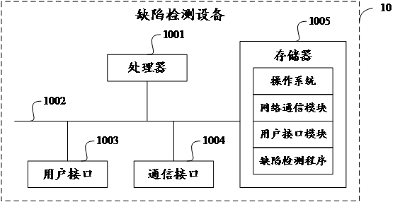
[0075] refer to figure 1 The schematic flowchart of the present invention presents the first embodiment of the defect detection method of the present invention. The defect detection method can be applied to a defect detection system, and specifically can be applied to the defect detection device 10 in the defect detection system.

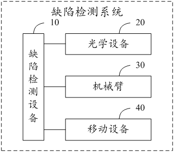
[0076] like figure 2 Shown is a schematic diagram of the structure of the defect detection system. The defect detection system can include:

[0077] an optical device 20 for performing optical processing on the LED chip to be tested, and the optical device 20 includes a laser transmitter;

[0078] The robotic arm 30 is used to move the second electrode to the LED chip to be tested;

[0079] a mobile device 40 for moving the LED chip to be tested; and,

[0080] The defect detection apparatus 10 is used for realizing the defect detection method.

[0081] Those skilled in the art can understand that, figure 2 The hardware structure shown in the ...

Embodiment 2

[0106] Based on the same inventive concept, on the basis of the first embodiment, a second embodiment of the defect detection method of the present invention is further proposed, and the method can also be applied to the defect detection device 10 in the above-mentioned defect detection system.

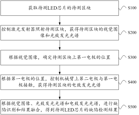
[0107] The defect detection method of this embodiment will be described in detail below with reference to the accompanying drawings and the above-mentioned defect detection system. The defect detection method may include the following steps:

[0108] Step S100 : acquiring the block to be tested of the LED chip to be tested.

[0109] Further, step S100 may include:

[0110] Step S110 : placing the LED chip to be tested including a plurality of blocks on the mobile device 40 .

[0111] like Figure 4 As shown, the mobile device 40 includes an XYZ stage 4002 and a precision turntable 4001 arranged on the XYZ stage 4002. The LED chip to be tested can be placed on the precision turntable ...

Embodiment 3

[0179] Based on the same inventive concept, refer to Figure 10 , proposes a first embodiment of the defect detection device of the present invention, which can be a virtual device and is applied to a defect detection system, and is specifically applied to the defect detection device 10 of the above-mentioned defect detection system.

[0180] Combine below Figure 10 The shown schematic diagram of the functional modules describes in detail the defect detection device provided in this embodiment, and the defect detection device may include:

[0181] The block acquisition module is used to acquire the block to be tested of the LED chip to be tested;

[0182] a synchronous acquisition module, used to control the laser transmitter to illuminate the block to be tested to obtain a visual image and photoluminescence spectrum of the block to be tested;

[0183] an electrode positioning module for determining the position of the first electrode on the block to be measured according t...


PUM


Abstract

The invention discloses a defect detection method, device and system and a storage medium, and relates to the technical field of semiconductor detection, and the method comprises the steps: obtaining a to-be-detected block of a to-be-detected LED chip; controlling a laser emitter to irradiate the to-be-detected block to obtain a visual image and a photoluminescence spectrum of the to-be-detected block; determining the position of a first electrode on the to-be-detected block according to the visual image; according to the position of the first electrode, a second electrode on the mechanical arm is controlled to make contact with the first electrode, and an electroluminescent spectrum of the to-be-detected block is obtained; and performing defect identification and result fusion according to the visual image, the photoluminescence spectrum and the electroluminescence spectrum to obtain a defect detection result of the to-be-detected LED chip. According to the invention, the problem of low detection efficiency of the defect detection of the Micro-LED chip in the prior art is solved, the purpose of carrying out defect detection on the LED chip by integrating visual detection, PL detection and EL detection is realized, and the defect detection efficiency of the LED chip is improved.

Description

technical field [0001] The present invention relates to the technical field of semiconductor inspection, and in particular, to a defect inspection method, device, system and storage medium. Background technique [0002] Micro Light Emitting Diode (Micro-LED) display technology refers to the self-luminous micron-scale light-emitting diode (Light Emitting Diode, LED for short) as the light-emitting pixel unit, which is assembled on the drive panel to form a high-density LED array display technology. Micro-LED chips refer to LED chips with a size less than 50*50um, which are small in size and high in integration. [0003] Defect inspection of Micro-LED chips generally refers to wafer inspection, which mainly includes three aspects, visual inspection, PhotoLuminescence (PL) inspection and Electro Luminescent (EL) inspection. In the current defect inspection of Micro-LED chips, the three inspection methods of visual inspection, PL inspection and EL inspection are carried out in...

Claims


Application Information

Patent Timeline
Patent Type & Authority Applications(China)
IPC IPC(8): G01N21/95G01N21/88G01N21/63G01N21/66G01R31/26G01R31/28G01R31/44G06T7/00G06V10/80
CPCG01N21/9501G01N21/8851G01N21/66G01N21/63G01R31/2601G01R31/2851G01R31/44G06T7/0004G01N2021/8887G06T2207/30108G06F18/25
Inventor 段江伟毕海汪伟张赫铭柯链宝
Owner JIHUA LAB
Why Eureka
Try Eureka