

Semiconductor bump defect detection method, electronic equipment and storage medium
A defect detection, semiconductor technology, applied in the field of defect detection
- Summary
- Abstract
- Description
- Claims
- Application Information
AI Technical Summary
Problems solved by technology
Method used
Image

Examples
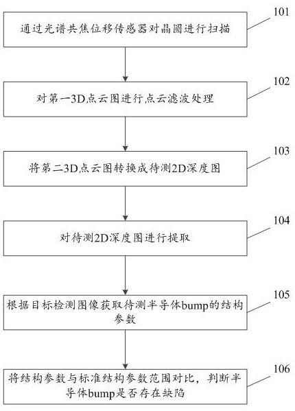
Embodiment 1
[0057] The current method for semiconductor bump defect detection is mainly based on laser line scan imaging. Laser line scan imaging is to project a laser line beam on the surface of the object to be tested through a laser transmitter, receive the reflected laser light through a photodetector, and then use a triangular The measurement method reconstructs the topography of the surface of the object to be measured, but in the above detection technology, some laser reflected beams cannot reach the imaging component due to the blocking of the concave corners of the surface of the object to be measured, resulting in partial positions on the surface of the object to be measured cannot be imaged , the detection accuracy will be affected by this, and the above detection technology is easily affected by the material on the surface of the object to be tested, and the laser emission module and the related imaging device are relatively complicated, which is not conducive to improving the d...
Embodiment 2
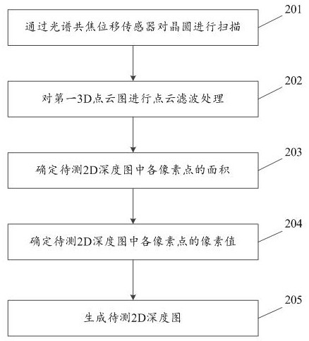
[0080] For ease of understanding, an embodiment of a semiconductor bump defect detection method is provided below for description. In practical applications, a 2D depth map to be tested is generated according to the area of each pixel point and the pixel value corresponding to each pixel point.
[0081] figure 2 This is a schematic flowchart of the second embodiment of the semiconductor bump defect detection method shown in the embodiment of the present application.
[0082] see figure 2 , the second embodiment of the semiconductor bump defect detection method shown in the embodiment of the present application includes:
[0083] 201. Scan the wafer through a spectral confocal displacement sensor;
[0084] In this embodiment of the present application, the specific content of step 201 is similar to the content of step 101 in the above-mentioned first embodiment, which is not repeated here.
[0085] 202. Perform point cloud filtering processing on the first 3D point cloud...
Embodiment 3
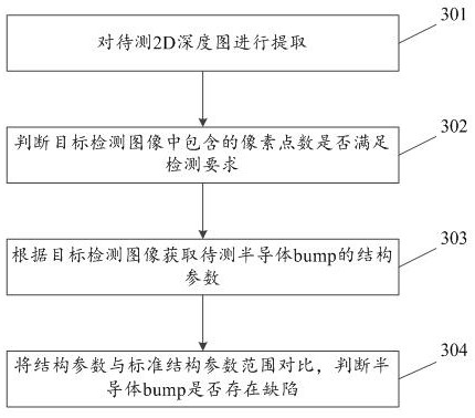
[0106] For ease of understanding, an example of a semiconductor bump defect detection method is provided below for illustration. In practical applications, each semiconductor bump is segmented and extracted for detection. By calculating the structural parameters of the semiconductor bump, it is judged whether there is a defect in the semiconductor bump .
[0107] image 3 It is a schematic flow chart of Embodiment 3 of the semiconductor bump defect detection method shown in the embodiment of the present application.
[0108] see image 3 , Embodiment 3 of the semiconductor bump defect detection method shown in the embodiment of the present application includes:
[0109] 301. Extract the 2D depth map to be measured;
[0110] The 2D depth map to be tested is binarized. In practical applications, the segmentation threshold can be adjusted according to the actual project to segment a single semiconductor bump, that is, the target detection image of the semiconductor bump to be ...
PUM
 Abstract
Description
Claims
Application Information