
Plasma confinement device and plasma treatment device

A plasma and confinement device technology, which is applied in the fields of plasma, semiconductor/solid-state device manufacturing, gaseous chemical plating, etc., can solve the problems of deposition, chamber particle contamination, shorten the service life of reaction chamber components, etc., and achieve constraining diffusion Effect

Active Publication Date: 2009-04-29
BEIJING NAURA MICROELECTRONICS EQUIP CO LTD
View PDF0 Cites 14 Cited by
  • Summary
  • Abstract
  • Description
  • Claims
  • Application Information

AI Technical Summary

Problems solved by technology

[0006] In the process of processing the silicon wafer 5, although most of the plasma will reside between the upper and lower electrodes, the plasma is diffused, and some of the plasma may diffuse into the entire reaction chamber. In the area where the plasma reaches, in the electric field, Under the action of the magnetic field, the plasma may corrode or deposit the components in the area at any time, which will cause particle pollution inside the chamber and may shorten the service life of the reaction chamber components

Method used


Image

  • Plasma confinement device and plasma treatment device
  • Plasma confinement device and plasma treatment device
  • Plasma confinement device and plasma treatment device

Examples


specific Embodiment 2

[0027] Specific embodiment two, such as image 3 , Figure 4 As shown, the through hole 8 is an elongated hole, and the direction of the elongated hole is perpendicular to the central axis of the plasma confinement device.

specific Embodiment 3

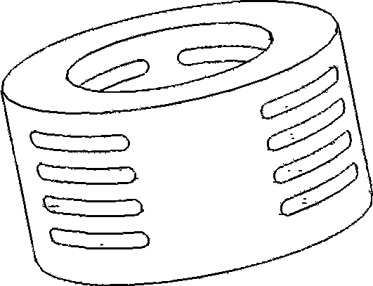
[0028] Specific embodiment three, such as Figure 5 , Figure 6 As shown, the through hole 8 is an elongated hole, and the direction of the elongated hole is parallel to the central axis of the plasma confinement device.

[0029] The direction of the elongated holes is not limited to the directions in Embodiment 2 and Embodiment 3, and may also be inclined to the central axis of the plasma confinement device.

[0030] The width of the elongated hole is 0.5-10 millimeters, can be 0.5, 1, 3, 6, 8, 10 millimeters, etc., and can also be other required sizes.

[0031] The shape of the through hole 8 is not limited to the above-mentioned circular hole and elongated hole, and may also be other regular or irregular shapes.

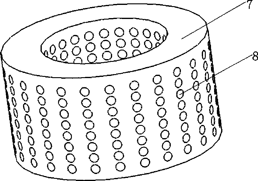
[0032] The sum of the cross-sectional areas of the plurality of through holes 8 is greater than or equal to 20% of the outer surface area of ​​the side wall 7 .

[0033] Such as Figure 7a , 7b , 7c, 7d, the shape of the through hole 8 can be an equal-diamete...


PUM


Abstract

The invention discloses a plasma restraint device and a plasma processing device. The plasma restraint device is of a hollow cylindrical shape; the side wall of the plasma restraint device is provided with a plurality of through holes; the depths of the through holes are larger than the average free path of the charged particles in the plasma; the through holes are round holes or elongated holes. The plasma restraint device is arranged between the upper electrode and the lower electrode of the plasma processing device and can move up and down. When sheet transmitting is carried out, the plasma restraint device is raised; when the sheet transmitting is stopped, the plasma restraint device is dropped to a proper position to prepare to start the technique. The plasma can be effectively restrained in a technical area between the upper electrode and the lower electrode to reduce the particle pollution of a reaction chamber and prolong the service life of the parts in a non-technique area.

Description

technical field [0001] The invention relates to semiconductor processing equipment, in particular to a plasma confinement device and a plasma processing device. Background technique [0002] Among semiconductor processing facilities, a plasma processing apparatus is one of main facilities. [0003] Plasma treatment devices in the prior art, such as figure 1 As shown, it includes a reaction chamber 1, an upper electrode 2, a lower electrode 3, an inner liner 4, a gas input device, a vacuum obtaining device (not shown in the figure) and the like. [0004] In the process of processing the silicon wafer 5, generally the upper electrode 2 is connected to a high-frequency RF (radio frequency) power supply, and the lower electrode 3 is connected to one or more RF power supplies. Generally, the RF frequency connected to the upper electrode is higher than that of the lower electrode. Electrode RF frequency. The process of the plasma processing device is generally: use the vacuum o...

Claims


Application Information

Patent Timeline
IPC IPC(8): H01L21/00H01L21/02H01L21/3065H01L21/31H01L21/205H01L21/285H01L21/67C23F4/00C23C16/513H01J37/32H05H1/00
Inventor 南建辉宋巧丽
Owner BEIJING NAURA MICROELECTRONICS EQUIP CO LTD
Learn More