Nozzle apparatus and semiconductor processing apparatus employing the nozzle apparatus

A nozzle device and semiconductor technology, applied in the field of microelectronics, can solve problems such as large dependence on external components, and achieve the effects of small dependence, easy installation and disassembly, and easy sealing

Active Publication Date: 2009-05-13
BEIJING NAURA MICROELECTRONICS EQUIP CO LTD
View PDF0 Cites 22 Cited by
  • Summary
  • Abstract
  • Description
  • Claims
  • Application Information

AI Technical Summary

Problems solved by technology

Therefore, in actual use, the nozzle device provided by the prior art is

Method used


Image

  • Nozzle apparatus and semiconductor processing apparatus employing the nozzle apparatus
  • Nozzle apparatus and semiconductor processing apparatus employing the nozzle apparatus
  • Nozzle apparatus and semiconductor processing apparatus employing the nozzle apparatus

Examples


Embodiment Construction

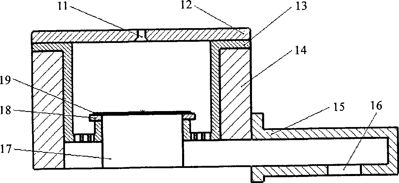
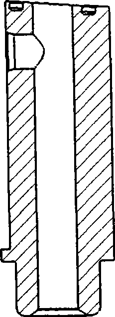
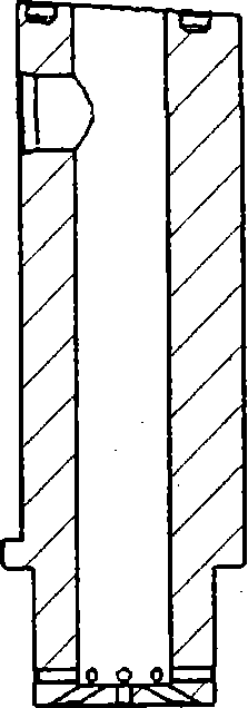
[0047] The technical core of the nozzle device provided by the present invention and the semiconductor processing equipment using the nozzle device is that by connecting the inlet part and the outlet part of the nozzle device into one body, and making the outlet part include a cavity connected to the inlet part, Therefore, the nozzle device is not only easy to assemble and disassemble and seal, but also has less dependence on external components; at the same time, it also makes the semiconductor processing equipment using the nozzle device easy to disassemble and seal. In addition, the nozzle device provided by the present invention and the semiconductor processing equipment using the nozzle device can make the gas entering the reaction chamber uniformly reach the surface of the processed / processed device such as a wafer, so that the processing / treatment of the processed / processed device surface The rate is uniform, which in turn leads to good machining / handling results.

[00...


PUM


Abstract

The invention provides a nozzle device which comprises a nozzle inlet part and a nozzle outlet part, and the nozzle outlet part is provided with an injection surface with an injection orifice, wherein, the nozzle outlet part is integrated with the nozzle inlet part and comprises a cavity connected with a the nozzle inlet for accommodating the fluid coming from the nozzle inlet part and leading the fluid to the injection nozzle, thereby enabling the injection hole to inject the fluid to the outside. Furthermore, the invention provides a semiconductor treatment device adopting the nozzle device. The nozzle device and the semiconductor treatment device which are provided by the invention have the advantages of facilitating assembly, disassembly and sealing, and low dependency on exterior parts. At the same time, the nozzle device and the semiconductor device can enable the gas to enter a reaction chamber and evenly reach devices to be processed/treated, such as a wafer and the like, so that the processing/treatment rate of the device surfaces to be processed/treated is uniform, and excellent processing/treating results can be further obtained.

Description

technical field [0001] The invention relates to the technical field of microelectronics, in particular to a nozzle device for jetting fluid and semiconductor processing equipment using the nozzle device. Background technique [0002] With the rapid development of electronic technology, people have higher and higher requirements for the integration of integrated circuits, which requires companies that produce integrated circuits to continuously improve the processing / processing capabilities of semiconductor devices. Currently, plasma etching techniques are widely used in the processing / handling of semiconductor devices. The so-called plasma etching technology refers to the ionization of the reactive gas under the excitation of radio frequency power to form a plasma containing a large number of active particles such as electrons, ions, excited atoms, molecules and free radicals. Various physical and chemical reactions occur on the surface of an object (for example, a wafer) a...

Claims


Application Information

Patent Timeline
IPC IPC(8): B05B1/14B05B15/00B05C11/10B05C11/11H01L21/00H01L21/3065
Inventor 刘少锋
Owner BEIJING NAURA MICROELECTRONICS EQUIP CO LTD
Why Eureka
Try Eureka