
Bolt lock device

A latching, current technology, applied in electrical components, logic circuits, pulse technology, etc., can solve the problems of increasing parasitic capacitance, the operating frequency can no longer be increased, and the current can no longer be increased, and the effect of avoiding the parasitic capacitance problem is achieved.

Active Publication Date: 2011-01-19
REALTEK SEMICON CORP
View PDF0 Cites 0 Cited by
  • Summary
  • Abstract
  • Description
  • Claims
  • Application Information

AI Technical Summary

Problems solved by technology

[0010] First of all, the first method is to increase the current without adjusting the aspect ratio (W / L ratio) of the internal transistor of the bias module, but this method will make the gate of the bias current source (usually a current mirror circuit) Drain voltage V DS Smaller, it may even cause the bias current source to enter the triode region (triode region), so that the current cannot be increased, and the operating frequency cannot be increased
[0011] The second method is to increase the current and adjust the aspect ratio of the internal transistor accordingly; however, this method will increase the parasitic capacitance seen from the gate terminal of the internal transistor; For a flip-flop, the added parasitic capacitance will be the load of the previous D-type flip-flop
In other words, the increased parasitic capacitance of the next-stage D-type flip-flop will increase the RC delay of the previous-stage D-type flip-flop, thereby limiting the maximum operating frequency of the overall circuit

Method used

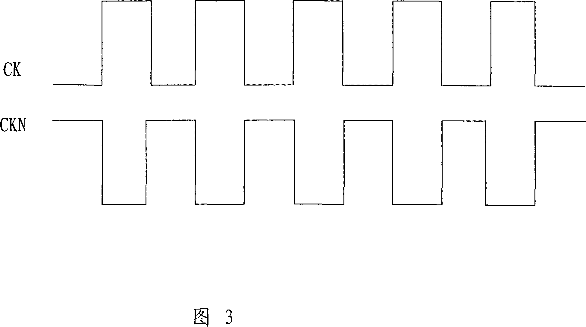

Image

  • Bolt lock device
  • Bolt lock device
  • Bolt lock device

Examples


Embodiment Construction

[0030] The present invention will be described in detail below with reference to the drawings.

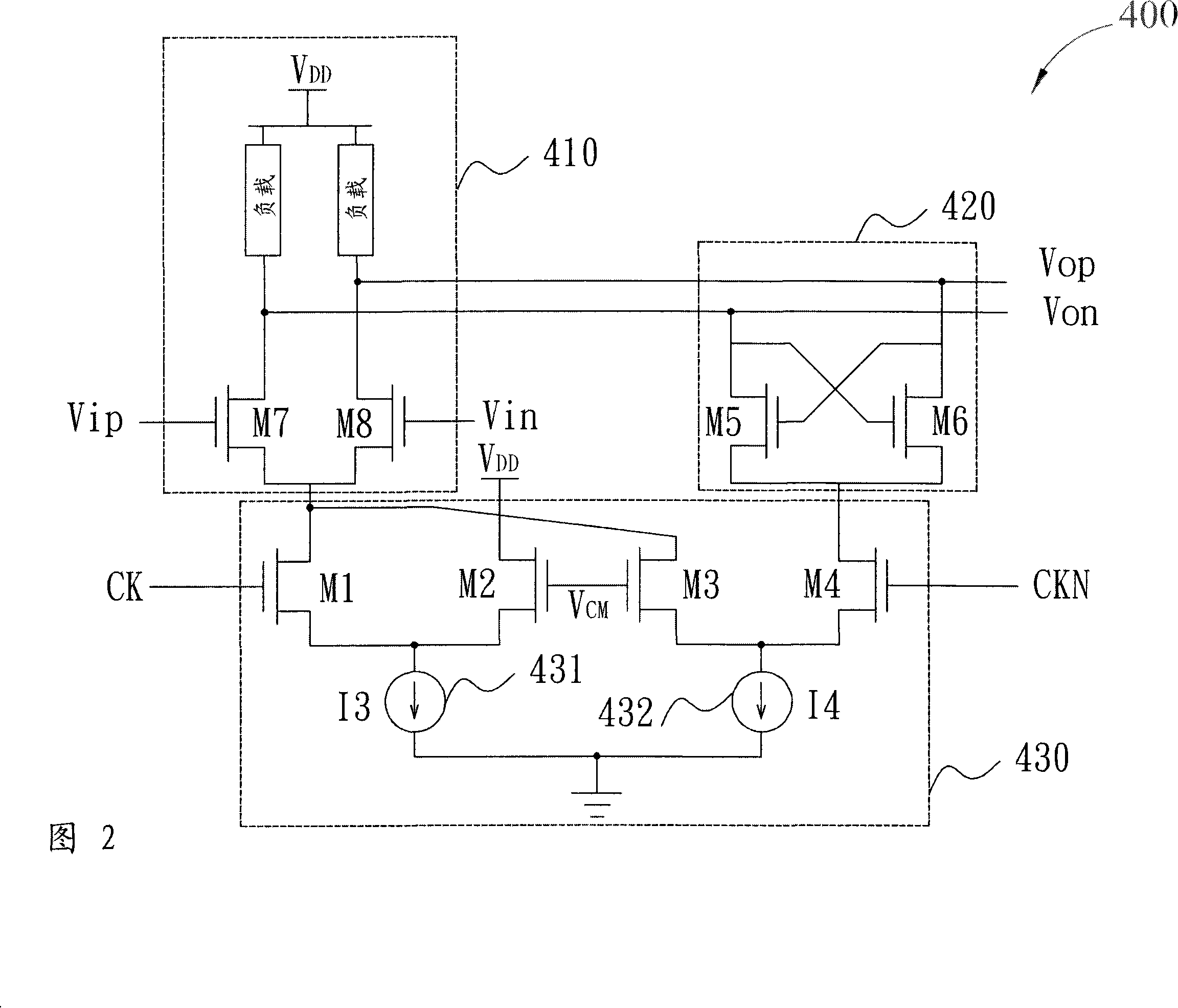
[0031] See here figure 2 , figure 2 It is a schematic diagram of the first embodiment of the latch 400 of the present invention. Such as figure 2 As shown, the latch 400 includes a preamplifier 410, a latch unit 420, and a bias circuit 430. Please note here that the pre-amplifier circuit 410 and the latch unit 420 have the same functions and operations as the aforementioned pre-amplifier circuit (pre-amplifier) ​​211 and the latch unit 212, so the details will not be repeated here. Operation.

[0032] For example, the latch unit 420 is composed of two cross-coupled transistors M5 and M6; since the gates of the transistors M5 and M6 are respectively coupled to the drains of each other, the reverse signal Von , Vop can be used to control the conduction state of transistors M5 and M6, thereby maintaining their own voltage level.

[0033] Please note that the bias circuit 430 of the lat...


PUM


Abstract

A latching device comprises an amplification circuit, a latching unit and a bias circuit. The amplification circuit is used for receiving a first bias current in a first state, so as to amplify an input signal and produce an amplified signal; the latching unit is used for latching the amplified signal and receiving a second bias current in a second state, so as to output the amplified signal; thebias circuit is used for supplying the first bias current to the amplification circuit, and supplying the second bias current to the latching unit; and the bias circuit comprises a first bias module used for supplying a third bias current to the amplification circuit in the first state, and a second bias module used for supplying a fourth bias current to the amplification circuit in the first state, wherein, the first bias current equals to the sum of the third bias current and the fourth bias current.

Description

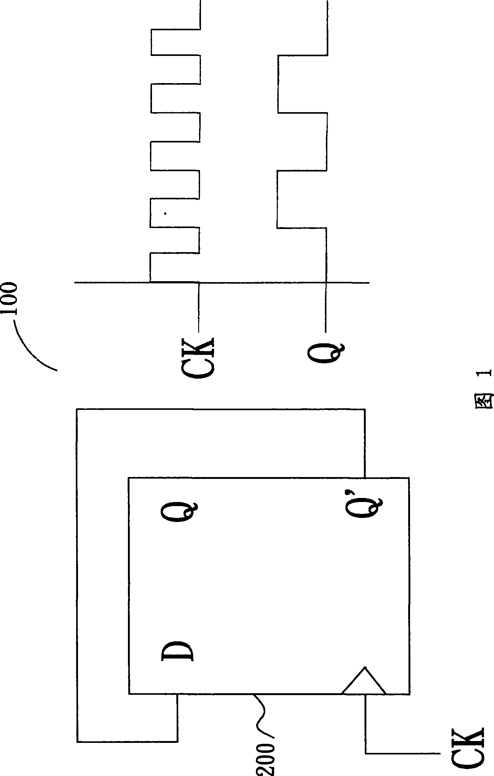
Technical field [0001] The invention relates to a latch, in particular to a latch capable of high-frequency operation. Background technique [0002] In integrated circuits, clock signals of different frequencies are often used to perform different operations; therefore, phase locked loop / synthesizers are widely used in the industry to produce different Frequency clock signal. [0003] As existing in the industry, the phase-locked loop / frequency synthesizer has a divider to divide the signal generated by its internal voltage-controlled oscillator, so that the feedback mechanism of the divider can be used to make The output of the phase-locked loop can generate a signal of the required frequency. [0004] Generally speaking, the frequency divider is usually implemented using D-type flip flops. See here figure 1 , figure 1 It is a schematic diagram of the existing frequency divider 100 with a divisor of 2. Such as figure 1 As shown, the frequency divider 100 is implemented by a D-ty...

Claims


Application Information

Patent Timeline
Patent Type & Authority Patents(China)
IPC IPC(8): H03K19/096H03K19/017
Inventor 邱伟茗陈家源
Owner REALTEK SEMICON CORP
Learn More