
CMOS image sensor pixel using a photodiode

An image sensor and charge technology, applied in the field of image sensors, can solve the problems of limiting pixel size, etc., and achieve the effects of eliminating threshold changes, floating diffusion changes, and low noise

Active Publication Date: 2009-05-20
OMNIVISION TECH INC
View PDF7 Cites 4 Cited by
  • Summary
  • Abstract
  • Description
  • Claims
  • Application Information

AI Technical Summary

Problems solved by technology

To maintain sensor performance, a large PD size and a minimum ratio (>30%) or fill factor between PD size and pixel size are required, which limits further reduction in pixel size

Method used


Image

  • CMOS image sensor pixel using a photodiode
  • CMOS image sensor pixel using a photodiode
  • CMOS image sensor pixel using a photodiode

Examples


Embodiment Construction

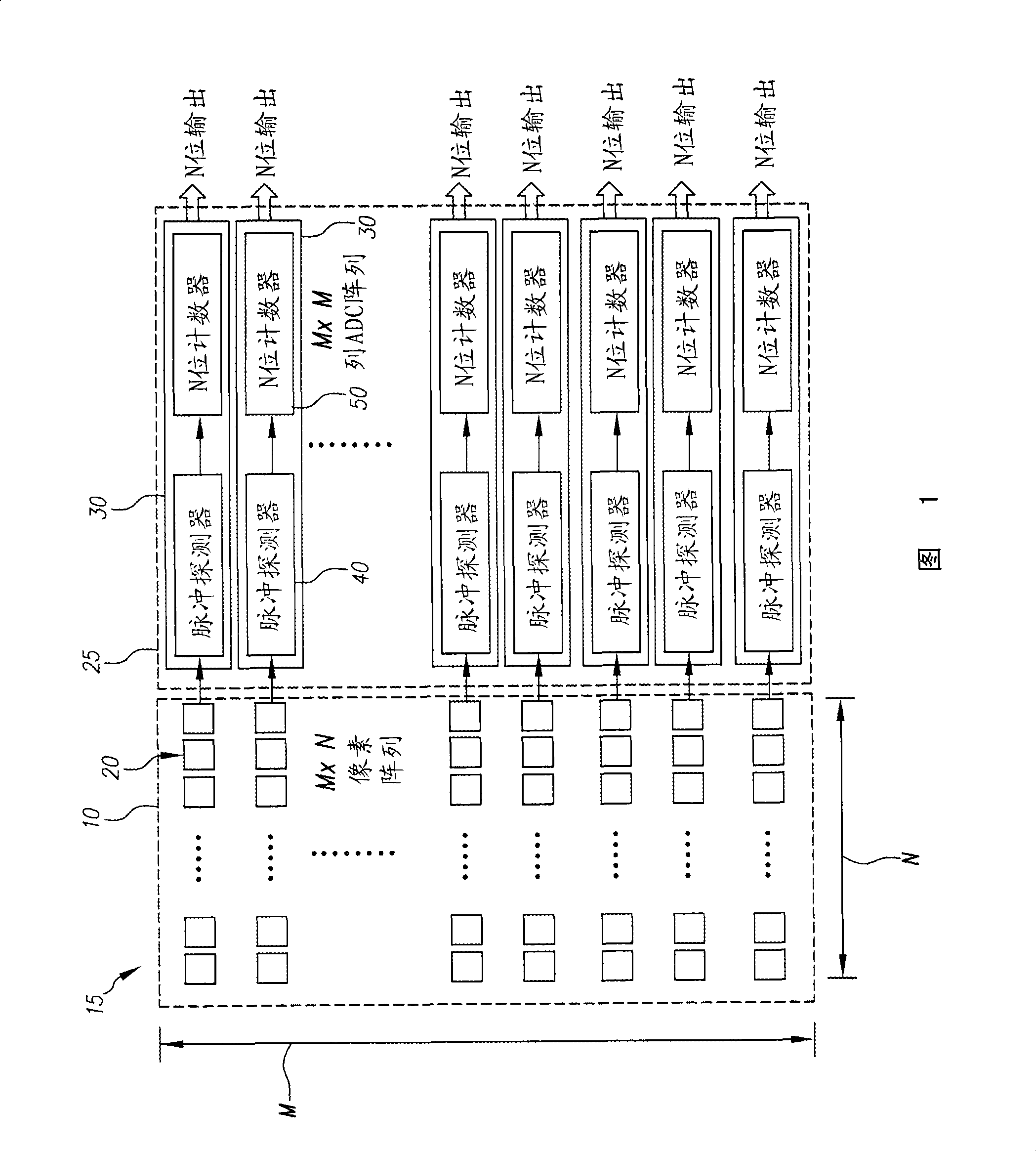
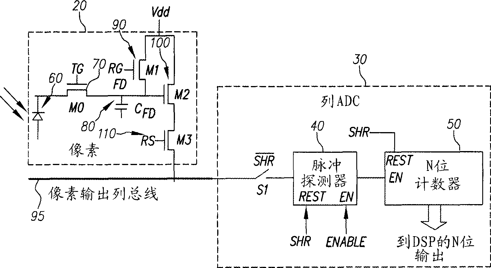
[0014] Referring to FIG. 1, there is shown a pixel array 10 of an image sensor 15 of the present invention. The pixel array 10 has a plurality of pixels 20 and a plurality of analog-to-digital converters 30, which are used for receiving and combining in a predetermined manner. The signals from the plurality of pixels 20 are stored. The analog-to-digital converter array 25 is connected to the output of the pixel array 10. The plurality of column analog-to-digital converters 30 includes an analog-to-digital converter array 25. A plurality of pulse detectors 40 are respectively connected to the pixel bus 95 (e.g. figure 2 Shown), and a plurality of counters 50 are respectively connected to the plurality of pulse detectors 40.

[0015] For a clear understanding, note that the above-mentioned device of the present invention limits the use of analog circuits (for the purpose of reducing noise and power consumption) and maximizes the use of the advantages of digital circuits. Also note ...


PUM


Abstract

An image sensor includes a photosensitive region that accumulates charge corresponding to received incident light; a transfer gate for transferring all or a portion of the charge from the photosensitive region; a voltage supply having an increasing voltage over time that is applied to the transfer gate; a floating diffusion for receiving the all or a portion of the charge from the photosensitive region and converting the charge to a voltage; an amplifier for receiving and amplifying a signal from the floating diffusion; a pulse detector for detecting a voltage pulse from the amplifier; and a counter for counting clock cycles between initiation of the increasing voltage until a signal is received from the detector which indicates initiation of charge transfer from the photosensitive region to the floating diffusion.

Description

Technical field [0001] The present invention generally relates to the field of image sensors, and more specifically, to a CMOS image sensor in which an image signal is converted into a digital signal immediately after being output from a pixel array. Background technique [0002] One of the trends of CMOS image sensors is the continuous scaling down of pixel size. Current CMOS image sensors all have the same or similar structure: the photosensitive device in each pixel, such as a photodiode FD and a photogate, is used to convert light signals into electrical signals, and charge into voltage. Floating diffusion (FD) capacitors , And an amplifier that buffers the floating diffusion capacitor from the large output bus capacitor and sends the electrical signal to the pixel array. The pixel output signal swing is initially determined by the FD capacitor and the amount of charge can be captured by the PD. The maximum amount of charge is proportional to the size of the photodiode. In or...

Claims


Application Information

Patent Timeline
Patent Type & Authority Applications(China)
IPC IPC(8): H04N3/15H04N5/357H04N5/374H04N5/378
CPCH04N5/353H04N5/378H04N5/3653H04N25/53H04N25/672H04N25/78H01L27/146H04N25/76H04N25/75
Inventor W·徐
Owner OMNIVISION TECH INC
Learn More