

A Level Restorer for Transmission Tube Selector
A technology of level restorer and selector, applied in the field of level restorer and structural design of high-speed circuits, can solve the problems of increasing delay, increasing area, etc. small effect
- Summary
- Abstract
- Description
- Claims
- Application Information
AI Technical Summary
Problems solved by technology
Method used
Image

Examples
Embodiment 1
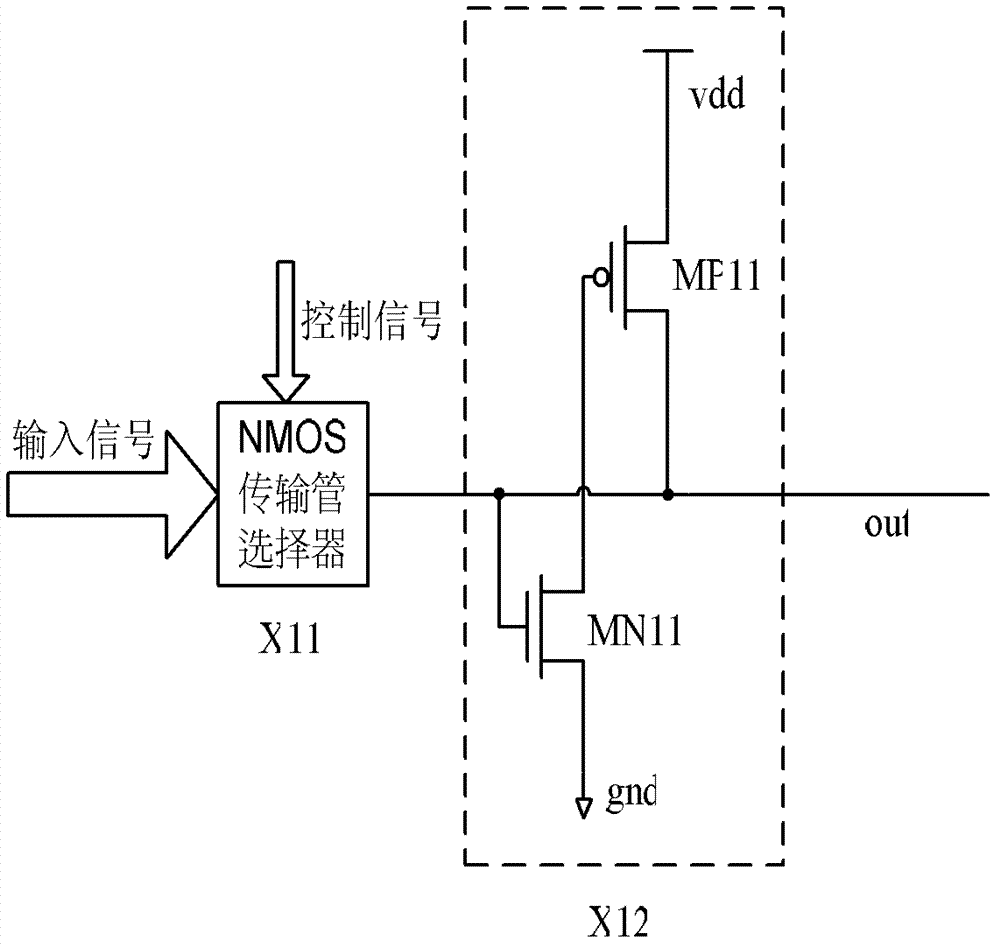
[0029] Example 1, such as figure 1 As shown, X11 is a one-level or N-level selector composed of NMOS transistors, the output terminal is out, and the level restorer X12 is composed of PMOS transistor MP11 and NMOS transistor MN11; the drain of MP11 is connected to the output terminal out of the selector , the source is connected to the power supply terminal vdd, the drain of MN11 is connected to the gate of MP11, the source is connected to the power supply terminal gnd, and the gate is connected to the output terminal out of the selector. When the selector is not working, the output terminal out will be quickly pulled up to high level by MP11 through the positive feedback loop of MN11 and MP11, thereby reducing the static power consumption of the subsequent CMOS circuit; when the N-level selector is working, the input When the signal flips from 0 to vdd, the out terminal can only be charged to vdd-N (vth), but through the positive feedback of MN11 and MP11, there will be no t...
Embodiment 2
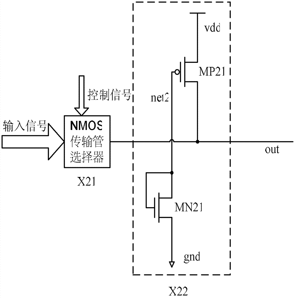
[0030] Example 2, such as figure 2As shown, X21 is a one-level or N-level selector composed of NMOS transistors, the output terminal is out, and the level restorer X22 is composed of PMOS transistor MP21 and NMOS transistor MN21; the drain of MP21 is connected to the output terminal out of the selector , the source level is connected to the power supply terminal vdd, the gate and drain of MN21 are connected and then connected to the gate of MP21, and the source level is connected to the power supply terminal gnd. When the selector is not working, the value of net2 will be pulled down to low level through the conduction of MN21, and the output terminal out will be quickly pulled up to high level by MP21, thereby reducing the static power consumption of the subsequent CMOS circuit; when N The stage selector works, when the input signal is flipped from 0 to vdd, the out terminal can only be charged to vdd-N (vth), but through the pull-up effect of MP21, there will be no threshol...
Embodiment 3
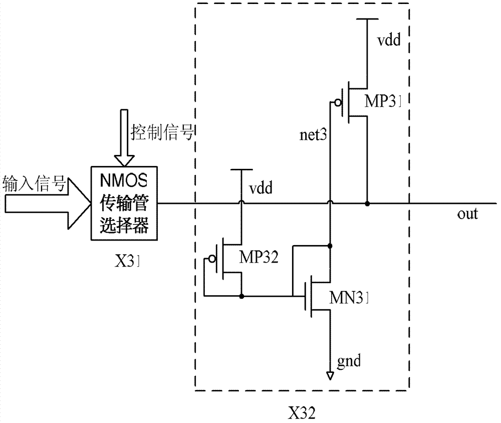
[0031] Example 3, such as image 3 As shown, X31 is a one-level or N-level selector composed of NMOS transistors, the output terminal is out, and the level restorer X32 is composed of NMOS transistors MN31 and PMOS transistors MP31 and MP32; the drain of MP31 is connected to the output of the selector Terminal out, the source level is connected to the power supply terminal vdd, the gate and drain of MN31 are connected to the gate of MP31, the source is connected to the power supply terminal gnd, the gate and drain of MP32 are connected to the gate of MN31, and the source is connected to the power supply terminal vdd. When the selector is not working, the value of net3 will be pulled to low level through the conduction of MN31, and the output terminal out will be quickly pulled up to high level by MP31, thereby reducing the static power consumption of the subsequent CMOS circuit; when N The level selector works, when the input signal is flipped from 0 to vdd, the out terminal ...
PUM
 Abstract
Description
Claims
Application Information