
Light-emitting device, electronic apparatus, and film-forming method

A technology of light-emitting device and film-forming method, which is applied in the direction of circuits, electrical components, electric solid devices, etc., to achieve the effect of stable potential and stable current control

Inactive Publication Date: 2009-06-10
SEIKO EPSON CORP
View PDF1 Cites 18 Cited by
  • Summary
  • Abstract
  • Description
  • Claims
  • Application Information

AI Technical Summary

Problems solved by technology

[0017] Moreover, the present invention also aims to solve the problems accompanying or related thereto.

Method used


Image

  • Light-emitting device, electronic apparatus, and film-forming method
  • Light-emitting device, electronic apparatus, and film-forming method
  • Light-emitting device, electronic apparatus, and film-forming method

Examples


Embodiment 1

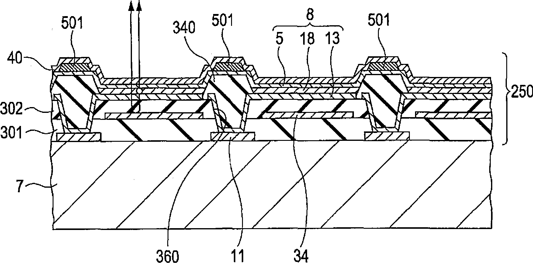
[0129] Auxiliary electrode width W=30μm

[0130] The thickness of the auxiliary electrode T = 310nm

[0131] Angle θ = 45 degrees for the conical shape

[0132] Auxiliary electrode material = aluminum

[0133] Thickness T1 of the barrier layer 40 = 200 nm

[0134] Material of barrier layer 40 = SiON

Embodiment 2

[0136] Auxiliary electrode width W=30μm

[0137] The thickness of the auxiliary electrode T = 200nm

[0138] Angle θ = 30 degrees for the conical shape

[0139] Auxiliary electrode material = silver

[0140] Thickness T1 of the barrier layer 40 = 200 nm

[0141] Material of barrier layer 40 = SiON

[0142] In the above-mentioned embodiments, the reason why the thickness of the auxiliary electrode can be reduced in the second embodiment compared with the first embodiment is that the resistance value of "silver" is smaller than that of "aluminum". In addition, the reason why the second embodiment can reduce the angle θ compared with the first embodiment is also for the same reason.

[0143] In any case, according to the above-mentioned Examples 1 and 2, it was confirmed that the effect according to the above-mentioned present embodiment is effectively exhibited.

[0144] A method of manufacturing the above-mentioned organic EL device, particularly a method of forming a film...


PUM

PropertyMeasurementUnit
angleaaaaaaaaaa

Abstract

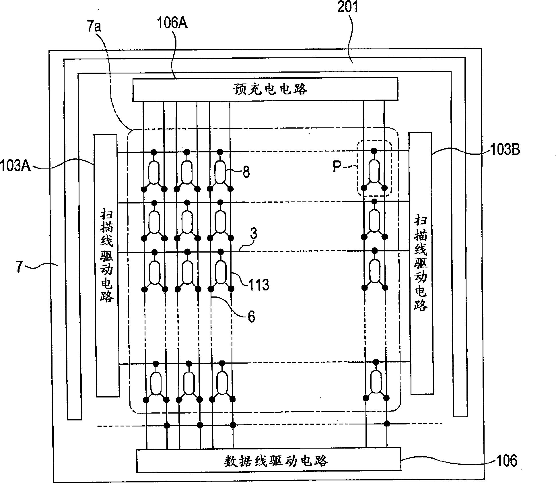
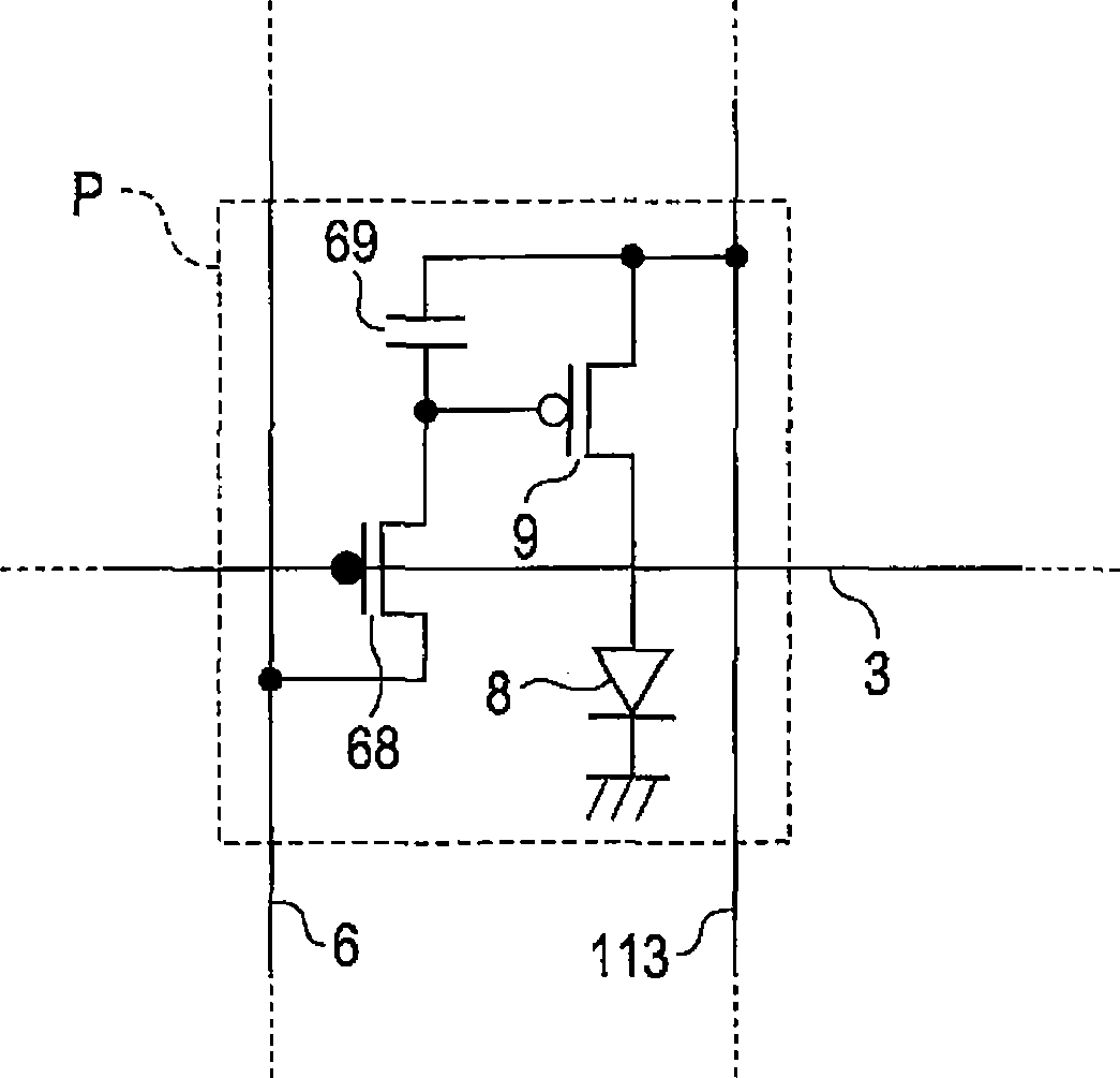
The present invention relates to a light-emitting device, electronic apparatus and film forming method. The light-emitting element includes: a pixel electric (13), a light-emitting function layer (18) and an organic EL element (8) of opposing electrode (5); an auxiliary electrode (501) formed on the opposing electrode with direction connection point with the opposing electrode; and a barrier layer (40) is formed so as to cover the auxiliary electrode and the opposing electrode, capable of preventing water and oxygen from penetrating into the organic EL element. In addition, the auxiliary electrode is in a strip shape extending in the first direction and has a cross section taken along the direction intersecting the first direction, having a shape including a tapered portion. Thus the organic EL element has long life.

Description

technical field [0001] The present invention relates to a light-emitting device and an electronic device that emit light by electroluminescence, and a preferred film-forming method suitable for their manufacture. Background technique [0002] OLED (organic light emitting diode: organic light emitting diode), that is, organic EL (electro luminescent: electroluminescence) element is provided as a thin and light-weight light emitting source. The organic EL element has a structure in which at least one organic thin film formed of an organic material is sandwiched between a pixel electrode and a counter electrode. In this case, the pixel electrode functions as an anode, and the counter electrode functions as a cathode, for example. When a current flows between the two, a current also flows to the above-mentioned organic thin film, whereby the organic thin film or the organic EL element emits light. In this case, since the intensity of the light emission corresponds to the magni...

Claims


Application Information

Patent Timeline
Patent Type & Authority Applications(China)
IPC IPC(8): H01L27/32H01L51/50H01L51/56H01L51/00C23C16/04C23C14/04
CPCH01L51/5221H01L51/5237H10K59/8052H10K59/873H10K2102/351H10K50/844H10K50/82
Inventor 新东晋四谷真一
Owner SEIKO EPSON CORP
Learn More