Thin-film type LED manufacturing method

A thin-film, p-type technology, applied in the direction of semiconductor devices, electrical components, circuits, etc., can solve problems such as unfavorable, short-circuit or leakage of positive and negative electrodes of LEDs, and low heat resistance of silver glue, so as to eliminate light and leakage, Reduce series resistance and ensure the effect of the process

Active Publication Date: 2010-11-17
DONGGUAN INST OF OPTO ELECTRONICS PEKING UNIV
View PDF2 Cites 0 Cited by
  • Summary
  • Abstract
  • Description
  • Claims
  • Application Information

AI Technical Summary

Problems solved by technology

However, the planarization process rarely uses conductive silver glue, because the silver glue filling on the side can easily lead to short circuit or leakage between the positive and negative electrodes of the LED.
The heat resistance of silver glue is low, which is not conducive to the preparation of nitrogen surface contact after peeling

Method used


Image

  • Thin-film type LED manufacturing method
  • Thin-film type LED manufacturing method
  • Thin-film type LED manufacturing method

Examples


Embodiment Construction

[0051] The preferred embodiment of the present invention will be described in more detail below with reference to the accompanying drawings of the present invention.

[0052] The preparation method of this embodiment comprises the following steps:

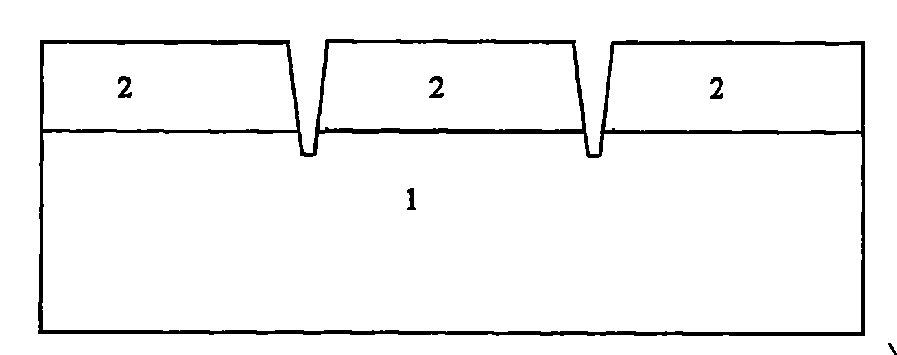
[0053] (1) if figure 1 As shown, a thick GaN-based LED epitaxial layer 2 of an n-type contact layer is grown on a sapphire substrate 1 with a thickness of 350-450 microns, and its thickness is 4-10 microns; The period is the size of the required LED chip, the scribing depth is greater than its thickness, and a certain angle is formed between the side wall of the groove formed by scribing and the substrate 1, and the angle range is 70-85°;

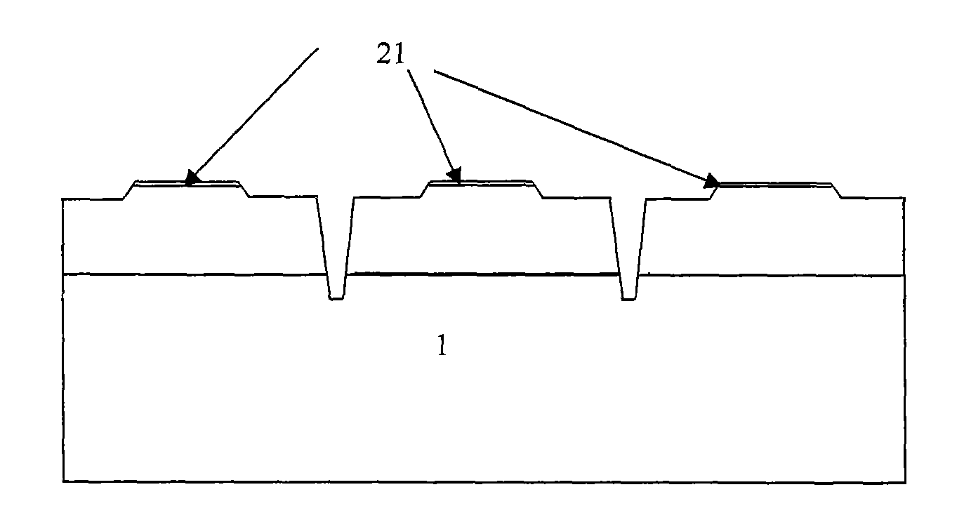
[0054] (2) if figure 2 As shown, reactive ion etching is used to form a trapezoidal mesa 21 on the surface of the epitaxial layer 2. The trapezoidal mesa 21 is located in the middle of the two scribing grooves. The bottom of the mesa reaches the n-GaN layer, and the thickness is between 0.6-...


PUM

PropertyMeasurementUnit
thicknessaaaaaaaaaa
heightaaaaaaaaaa
thicknessaaaaaaaaaa

Abstract

The invention discloses a method for preparing a thin-film LED, which belongs to the technical field of preparing semiconductor chips. The method comprises the steps of obtaining a wedge-shaped groove through laser scribing on an epitaxial layer; utilizing reactive ion etching to obtain a P-type trapezoidal mesa with an oblique side; preparing a p-type ohmic contact and a reflecting electrode on the trapezoidal mesa; preparing an insulation-passivation layer on the rest part except the electrode of the trapezoidal mesa; uniformly coating the whole LED epitaxial layer and a substrate with an appropriate amount of conductive silver colloid with high thermal conductivity as well as matched expansion coefficient and elastic modulus; subjecting a sapphire substrate to laser peeling after high-temperature bonding; cleaning a surface; forming an n electrode on the surface; roughening a light-outlet surface except the electrode; thinning the substrate to a needed thickness; preparing an ohmiccontact and an eutectic weld pad on the back of the substrate; performing laser scribing and cracking and obtaining a thin-film LED chip. The method has the advantages of reducing chip rupture brought by laser peeling, increasing the outgoing of ambient light of the chip, increasing bonding strength and improving the light-emitting efficiency and reliability of the chip.

Description

technical field [0001] The invention relates to a thin-film LED, in particular to an LED preparation method for transferring a GaN-based LED epitaxial film to a heat-conducting substrate by peeling off a sapphire substrate by laser, and belongs to the technical field of semiconductor chip preparation. Background technique [0002] In the traditional fabrication method of front-mount LEDs, GaN-based LEDs are usually grown on a sapphire substrate. Due to the poor insulation and thermal conductivity of sapphire, both the positive and negative electrodes of the LED chip must be prepared on the chip, and the resulting chip has a high operating temperature. . One main method to solve the above-mentioned problems is to remove the sapphire substrate by the laser lift-off (LLO) method. In order to achieve this goal, the LED electrodes must first be prepared, and then the epitaxial layer is bonded to a thermally and electrically conductive semiconductor wafer or a metal substrate or ...

Claims


Application Information

Patent Timeline
Patent Type & Authority Patents(China)
IPC IPC(8): H01L33/00
Inventor 陈志忠齐胜利孙永健田朋飞康香宁秦志新于彤军张国义
Owner DONGGUAN INST OF OPTO ELECTRONICS PEKING UNIV
Why Eureka
Try Eureka