Thermal vapor bubble type ink jet head chip structure and method for producing the same

A chip structure and manufacturing method technology, applied in printing and other directions, can solve problems such as inconvenience, borophosphosilicate glass brittleness, and general products and methods without suitable structures and methods, so as to reduce costs, increase service life, and reduce heat. The effect of the shock effect

Inactive Publication Date: 2009-06-17
INT UNITED TECH
View PDF4 Cites 3 Cited by
  • Summary
  • Abstract
  • Description
  • Claims
  • Application Information

AI Technical Summary

Problems solved by technology

This borophosphosilicate glass material has a serious stress problem. When the borophosphosilicate glass encounters the high temperature of the resistance layer at work, it will be more likely to cause brittle cracks in the borophosphosilicate glass and affect the service life of the inkjet head chip.
[0005] It can be seen that the above-mentioned existing inkjet head chip structure and its manufacturing method obviously still have inconvenience and defects in

Method used


Image

  • Thermal vapor bubble type ink jet head chip structure and method for producing the same
  • Thermal vapor bubble type ink jet head chip structure and method for producing the same
  • Thermal vapor bubble type ink jet head chip structure and method for producing the same

Examples


Embodiment Construction

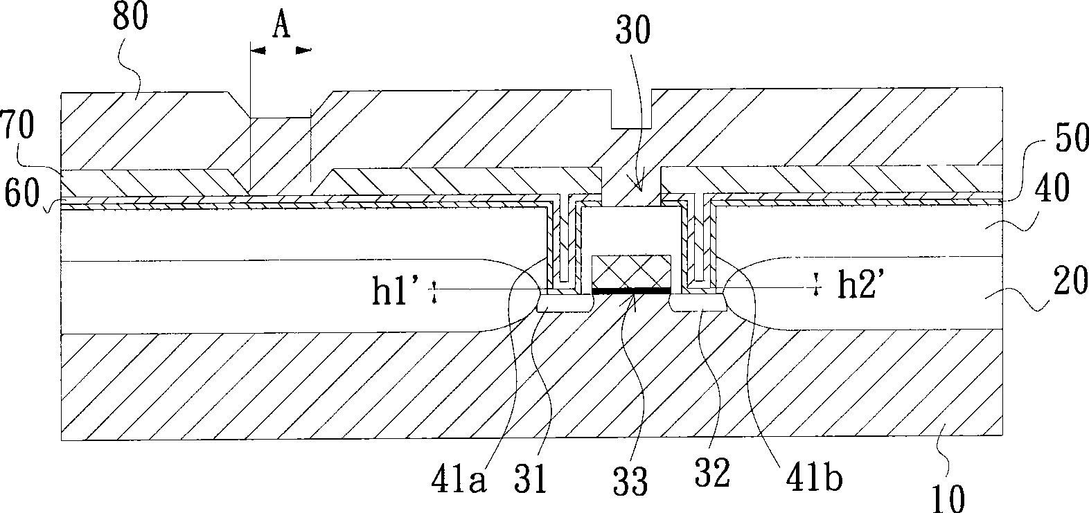
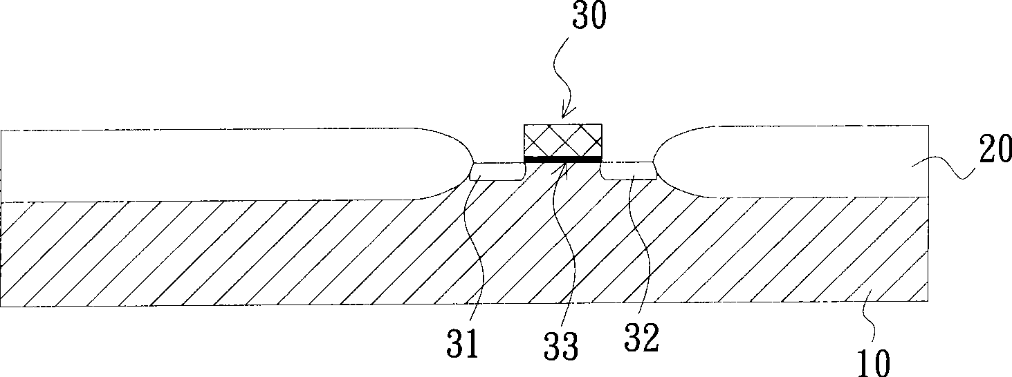
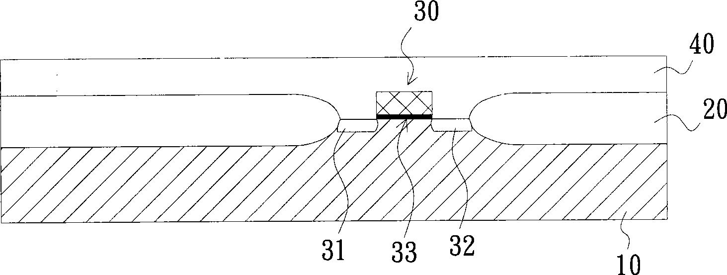
[0059] For further elaborating the technical means and effect that the present invention takes for reaching the intended invention purpose, below in conjunction with accompanying drawing and preferred embodiment, to the thermal bubble type ink-jet head chip structure that proposes according to the present invention and its manufacturing method its specific Embodiments, structures, methods, steps, features and effects thereof are described in detail below.

[0060] Other purposes and advantages of the present invention can be further understood from the technical features disclosed in the present invention. The aforementioned and other technical contents, features and effects of the present invention will be clearly presented in the following detailed description of preferred embodiments with reference to the drawings. Through the description of the specific implementation mode, when the technical means and functions adopted by the present invention to achieve the predetermined...


PUM

PropertyMeasurementUnit
Lengthaaaaaaaaaa
Widthaaaaaaaaaa
Thicknessaaaaaaaaaa

Abstract

The invention relates to a thermal bubble inkjet head chip structure and a method for manufacturing the same. The thermal bubble inkjet heat chip structure comprises a basal layer, an oxidation layer and a driving circuit, a dielectric layer, a source electrode and a drain electrode, a cushion layer, a resistance layer, a conductive layer and a protective layer, wherein the oxidation layer and the driving circuit are formed above the basal layer, the driving circuit is enclosed by the oxidization layer, the dielectric layer is formed above the driving circuit, the source electrode and the drain electrode are exposed in the driving circuit, the cushion layer is formed above the dielectric layer and covers the driving circuit and the drain electrode, the resistance layer is formed above the cushion layer and is provided with a heating area, the conductive layer is covered on the resistance layer partially and the protective layer is formed above the conductive layer and above the heating area. The cushion layer added between the dielectric layer and the resistance layer can cushion instant high temperature generated in the resistance layer, reduce the heat impact effect withstood by the dielectric layer below the heating layer and consequently improve the service life of the inkjet heat chip.

Description

technical field [0001] The invention relates to an inkjet head chip structure and a manufacturing method thereof, in particular to a thermal bubble type inkjet head chip structure capable of buffering instantaneous high temperature generated by a resistance layer and a manufacturing method thereof. Background technique [0002] Many thermal bubble inkjet head chip technologies have been disclosed. For example, the thermal bubble inkjet head chip structure disclosed in U.S. Patent No. 5,122,812 includes a substrate layer and an insulating oxide layer. layer), and then form a resistive layer on the base layer and be directly electrically connected with the source (source) and the drain (drain) in the driver circuit. Then a conductive metal layer is formed on part of the resistance layer, and the area of ​​the resistance layer not covered by the conductive metal layer is a heating area. When the driving circuit operates, the heating area in the chip structure of the inkjet hea...

Claims


Application Information

Patent Timeline
IPC IPC(8): B41J2/14B41J2/16B41J2/05
Inventor 李致淳赖伟夫李明玲
Owner INT UNITED TECH
Why Eureka
Try Eureka