Touch screen and display device
一种显示装置、触摸屏的技术,应用在绝缘载体上的导电层、纳米技术、仪器等方向,能够解决阻值分布不均匀、线性及准确性差、透明度下降等问题,达到提高分辨率和精确度、好韧性和机械强度、均匀阻值分布的效果
- Summary
- Abstract
- Description
- Claims
- Application Information
AI Technical Summary
Problems solved by technology
Method used
Image
Examples
preparation example Construction
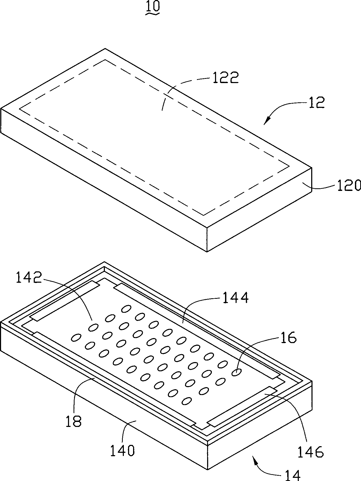
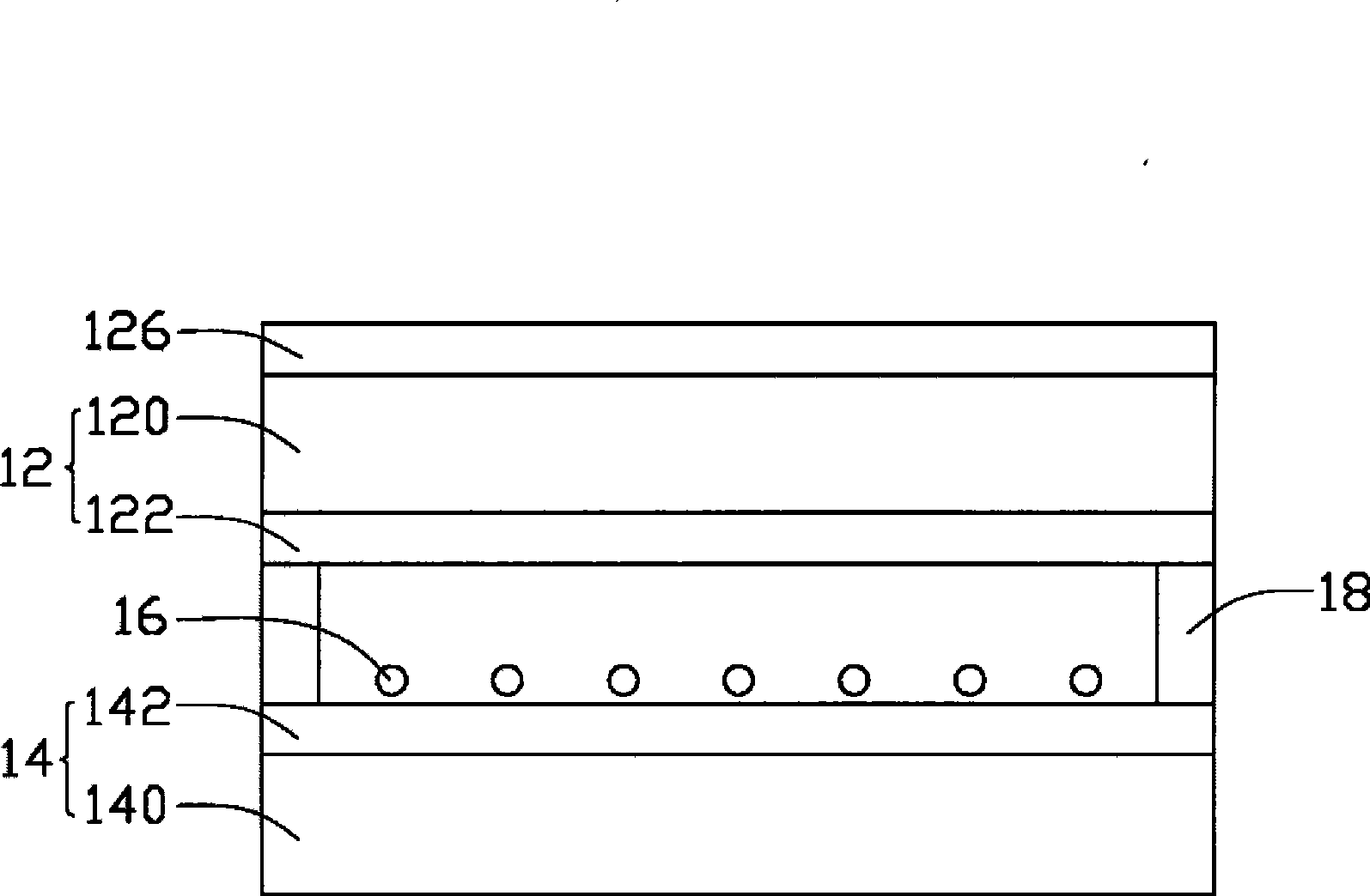
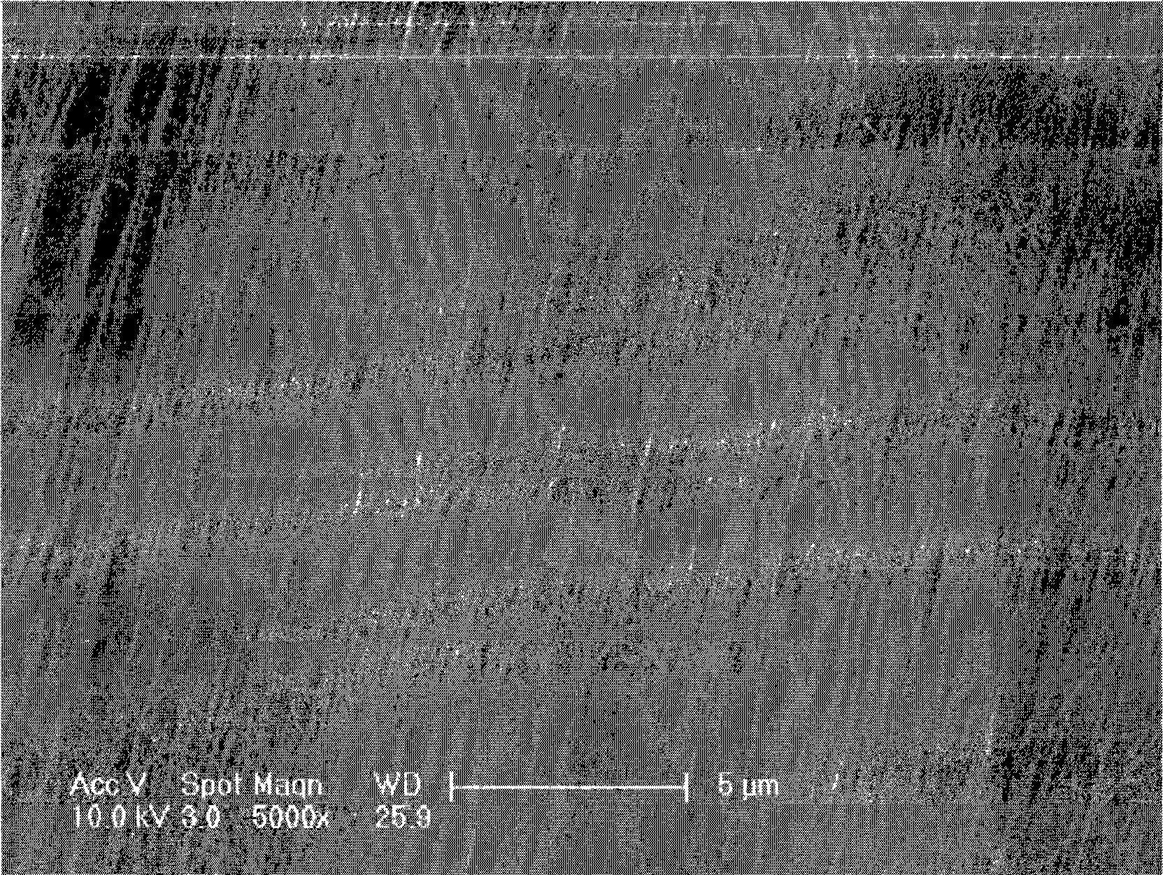
[0024] The preparation method of the ordered carbon nanotube film used in the first conductive layer 122 and the second conductive layer 142 of this embodiment mainly includes the following steps:
[0025] Step 1: providing a carbon nanotube array, preferably, the array is a super-aligned carbon nanotube array.
[0026] The carbon nanotube array provided in the embodiment of the technical solution is a single-wall carbon nanotube array, a double-wall carbon nanotube array or a multi-wall carbon nanotube array. In this embodiment, the preparation method of the super-parallel carbon nanotube array adopts the chemical vapor deposition method, and its specific steps include: (a) providing a flat substrate, which can be a P-type or N-type silicon substrate, or a silicon substrate formed with The silicon base of oxide layer, present embodiment preferably adopts the silicon base of 4 inches; (b) uniformly form a catalyst layer on the base surface, this catalyst layer material can be ...
PUM
| Property | Measurement | Unit |
|---|---|---|
| width | aaaaa | aaaaa |
| diameter | aaaaa | aaaaa |
| diameter | aaaaa | aaaaa |
Abstract
Description
Claims
Application Information
 - R&D
- Intellectual Property
- Life Sciences
- Materials
- Tech Scout
- Unparalleled Data Quality
- Higher Quality Content
- 60% Fewer Hallucinations
Browse by: Latest US Patents, China's latest patents, Technical Efficacy Thesaurus, Application Domain, Technology Topic, Popular Technical Reports.
© 2025 PatSnap. All rights reserved.Legal|Privacy policy|Modern Slavery Act Transparency Statement|Sitemap|About US| Contact US: help@patsnap.com


