
Liquid crystal display panel and its test method

A technology of a liquid crystal display panel and a test method, which is applied in the directions of measuring electricity, measuring devices, measuring electrical variables, etc., can solve the problems of slow test speed, electrode scratches, and rapid probe consumption, and achieves low cost, high reliability, and high reliability. Test the effect of fast speed

Active Publication Date: 2009-06-24
SHENZHEN SUCCESS ELECTRONICS LTD
View PDF0 Cites 11 Cited by
  • Summary
  • Abstract
  • Description
  • Claims
  • Application Information

AI Technical Summary

Problems solved by technology

Because the vertical conductive strip conducts electricity by the conductive substance in the strip, a certain gap needs to be ensured between the conductive substances, generally more than 50 microns, so it is not possible to effectively test all defects for products with an electrode spacing of less than 50 microns
In recent years, vertical conductive strips with smaller gaps between conductive materials have been developed, but because of their high cost, insufficient test reliability and durability, they are difficult to be used in large-scale production of liquid crystal displays
[0007] There are also instruments that use probe scanning to test the electrical performance defects of this type of liquid crystal display panel, but because they rely on metal probe contact scanning, it is easy to cause scratches on the electrodes, and at the same time, the consumption of probes is fast, the cost is high, and the test speed is slow. , generally only used for sampling testing, it is difficult to achieve large-scale testing of products to ensure zero-defect product shipments
[0008] There is also an instrument that uses the image contrast method to test the electrode defects of the liquid crystal display panel. This method is generally applicable to the test of a single liquid crystal display panel. For the liquid crystal display panel after the box, it is impossible to test the short circuit between electrodes and the electrode of the integrated circuit packaging area. Defects

Method used


Image

  • Liquid crystal display panel and its test method
  • Liquid crystal display panel and its test method
  • Liquid crystal display panel and its test method

Examples


Embodiment 1

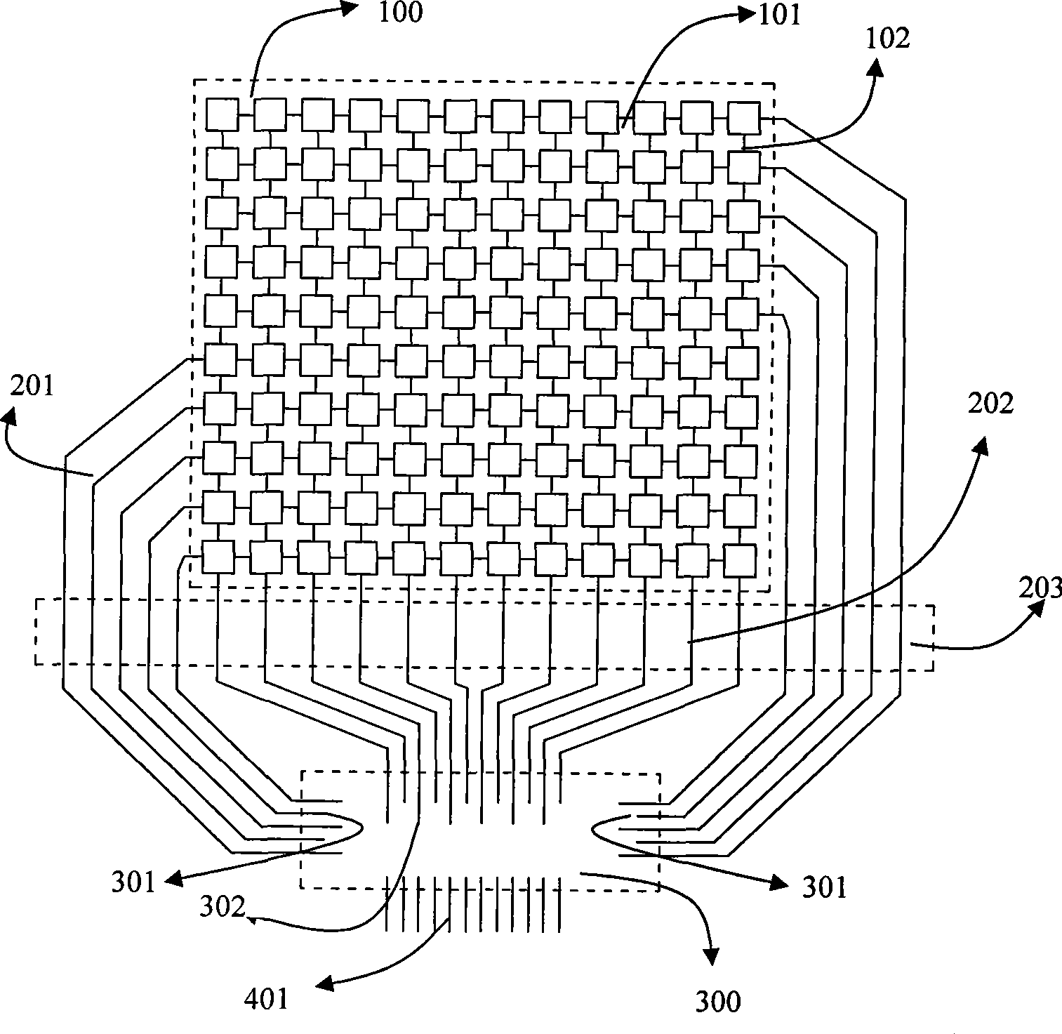
[0059] Form row electrodes 101 and column electrodes 102 on the panel, connect the column electrodes with the design electrodes of the integrated circuit packaging area 300, and connect the connection lines between the row electrodes and the integrated circuit packaging area from the left and right respectively according to the upper and lower screens of the display area. Under the circuit packaging area, extend the distance between the row and column electrodes and the connecting wires of the integrated circuit, the odd-numbered rows or columns or the even-numbered rows or columns.

[0060] The test is divided into two steps:

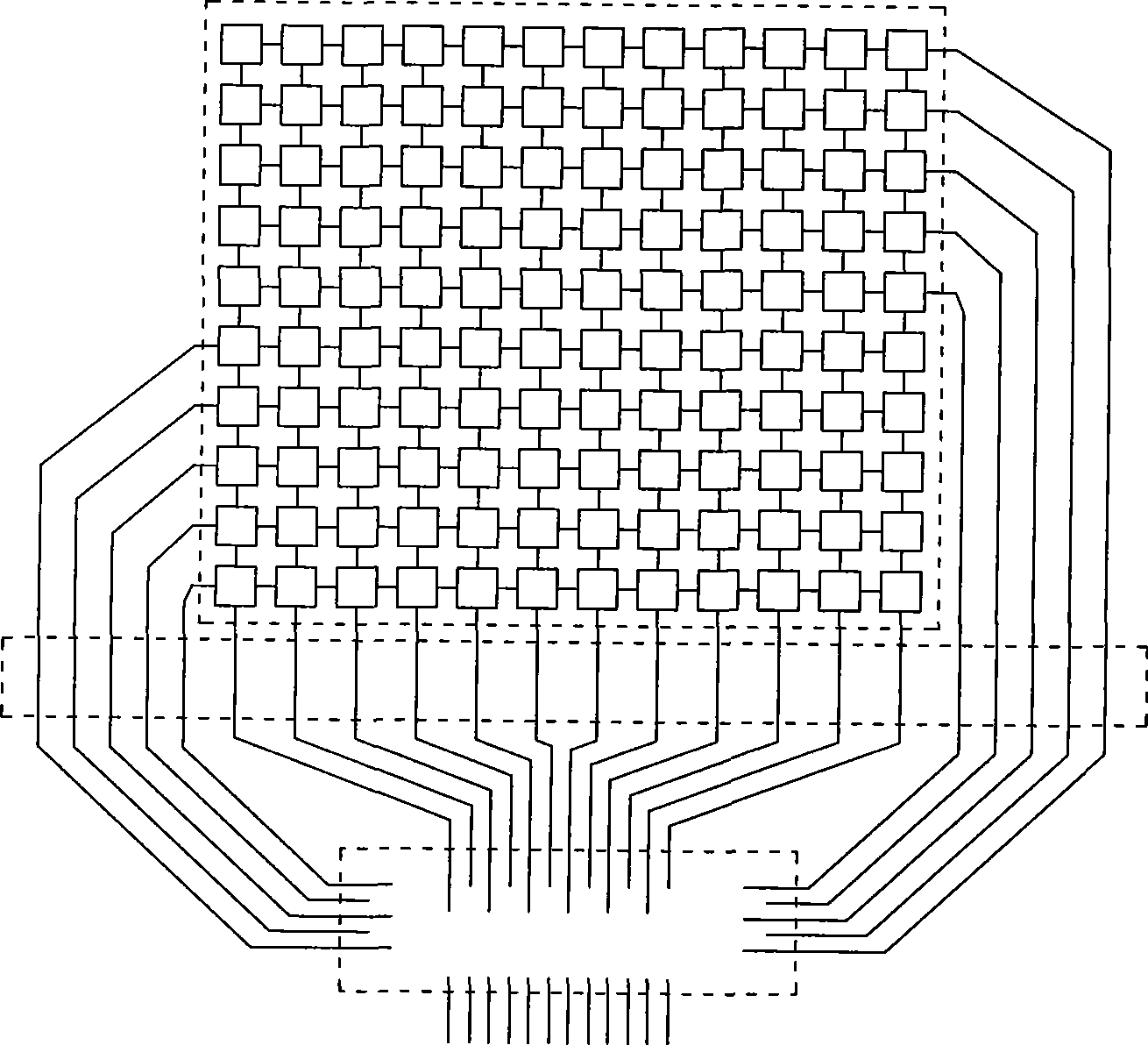
[0061] When no voltage is applied, all dot matrixes, that is, the intersections of row electrodes and column electrodes, have no display patterns, such as figure 2 As shown, this figure is for comparison with the pattern shown.

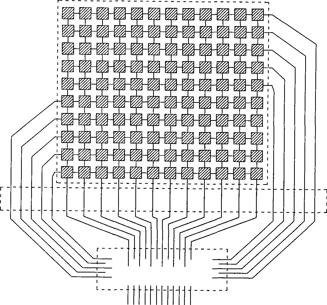
[0062] The first step is to apply AC voltage to all selected test areas 203 and observe under crossed polarizers. The resul...

Embodiment 2

[0071] Row electrodes 101 and column electrodes 102 are formed on the panel, and the column electrodes are connected to the design electrodes of the integrated circuit packaging area 300. The connection lines between the odd-numbered rows of the row electrodes and the integrated circuit packaging area are drawn from the side of the display area, and the even-numbered rows are connected to the integrated circuit packaging area. The connection lines of the packaging area are drawn from the other side of the display area. Under the integrated circuit packaging area, the connection wires between the column electrodes and the integrated circuit are extended (odd-numbered rows (columns) or even-numbered rows (columns) are extended), and the connection wires between the row electrodes and the integrated circuit do not need to be extended at intervals.

[0072] The test is divided into two steps:

[0073] The first step is to apply AC voltage to all selected test areas 203 and observe...


PUM


Abstract

The invention provides a liquid crystal display panel which comprises a line electrode, a column electrode, connecting lines, an auxiliary testing electrode and an integrated circuit input electrode; the line electrode is formed on a base plate; the column electrode is formed on the base plate and is perpendicular to the line electrode, wherein, an LCD display area is formed commonly by the line electrode and the column electrode; the connecting lines are arranged between the line electrode and an integrate circuit and between the column electrode and the integrate circuit, wherein, a fully-selected testing area is formed by the line electrode, the column electrode and the connecting lines of the integrate circuit; the auxiliary testing electrode is positioned under the encapsulation area of the integrate circuit and comprises a line auxiliary testing electrode and a column auxiliary testing electrode; and the integrated circuit input electrode is formed on the base plate. The method comprises the following steps: firstly, applying static, square wave or sine wave drive signals to the fully-selected testing area formed by the line electrode, the column electrode and the connecting lines of the integrate circuit and displaying all lattices in the display area, namely fully-displaying test; and secondly, applying static, square wave or sine wave drive signals to a partially-displaying test circuit under the encapsulation area of the integrate circuit and displaying half lattices at intervals in the display area, namely partially-displaying test.

Description

technical field [0001] The invention relates to the technical field of liquid crystal display, in particular to a liquid crystal display panel and a testing method thereof. Background technique [0002] A liquid crystal display (LCD) includes two liquid crystal display panels, a dielectrically anisotropic liquid crystal layer between the two liquid crystal display panels, and a polarizing layer outside the two liquid crystal display panels. [0003] Currently, liquid crystal display panels that are widely used are generally divided into active liquid crystal display panels and passive liquid crystal display panels. The active liquid crystal display panel mainly refers to the thin film transistor liquid crystal display, and its display unit controls the grayscale display through independent transistors. The passive display panel mainly controls the liquid crystal display unit to realize the grayscale display through mutually insulated row electrodes for selecting liquid crys...

Claims


Application Information

Patent Timeline
Patent Type & Authority Applications(China)
IPC IPC(8): G02F1/13G01R31/00
Inventor 杨顺林宋宇红黄清华
Owner SHENZHEN SUCCESS ELECTRONICS LTD
Learn More