Electro-optical device and electronic apparatus

An electro-optical device and electrode technology, which is applied in the direction of circuits, electrical components, and electrical solid devices, can solve problems such as difficulty in expanding the effective range, prolonging manufacturing time, and reducing yields

Active Publication Date: 2009-07-15
138东液晶显示器发展有限公司
View PDF1 Cites 12 Cited by
  • Summary
  • Abstract
  • Description
  • Claims
  • Application Information

AI Technical Summary

Problems solved by technology

However, reducing the thickness of the glass substrate will lead to a decrease in the strength of the substrate, which will lead to many disadvantages such as lower yield, longer manufacturing time, and lower quality.
[0012] That is, in conventional display devices, there is an unsolved problem that it is difficult to expand the effective range.

Method used


Image

  • Electro-optical device and electronic apparatus
  • Electro-optical device and electronic apparatus
  • Electro-optical device and electronic apparatus

Examples


Embodiment Construction

[0094] Embodiments will be described with reference to the drawings, taking a display device using an organic EL device as an electro-optical device as an example.

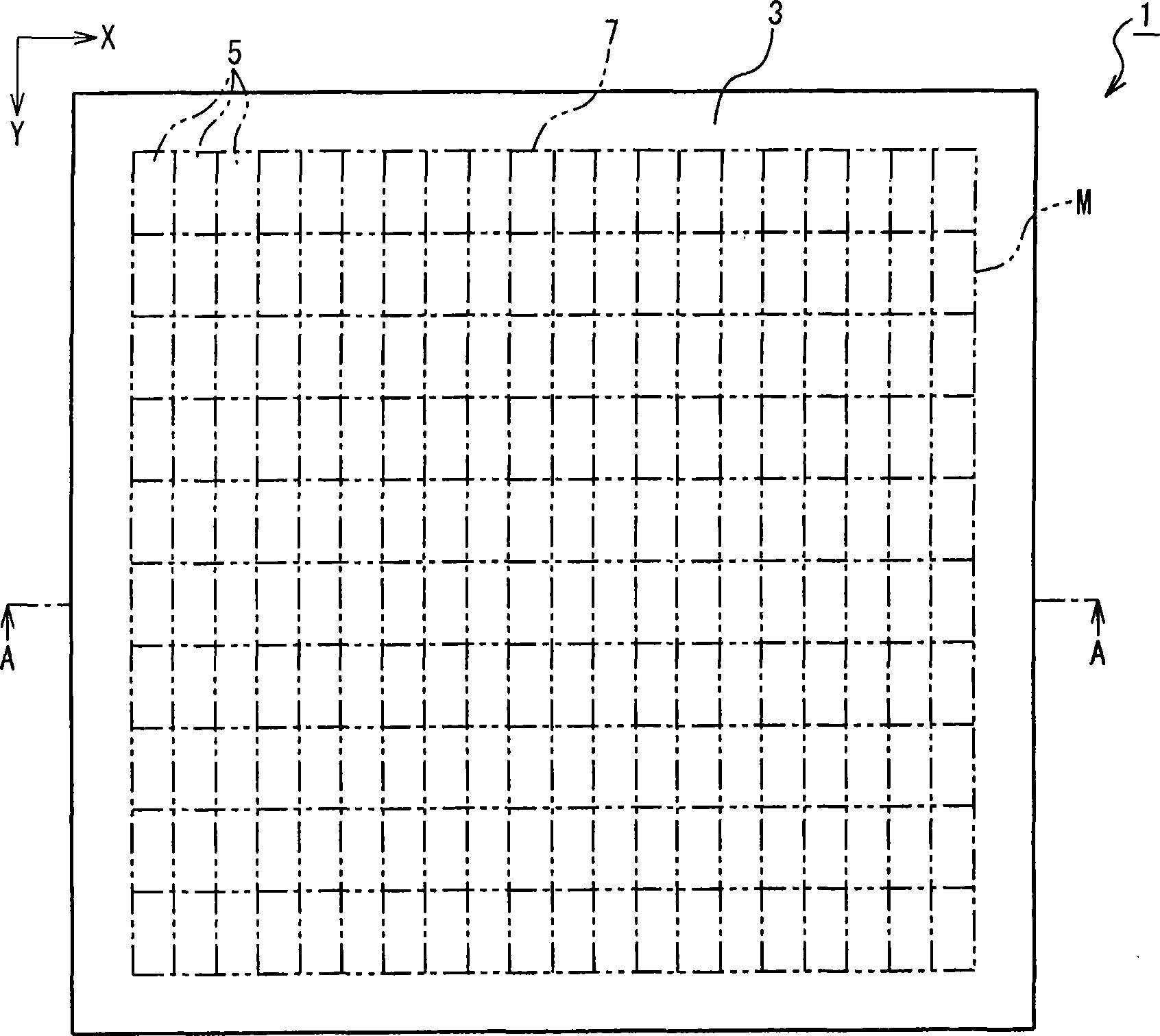
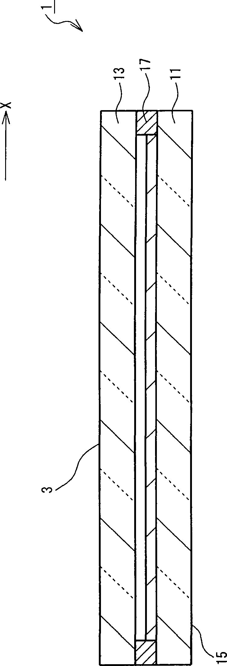
[0095] Such as figure 1 As shown, the display device in Embodiment 1 has a display surface 3 .

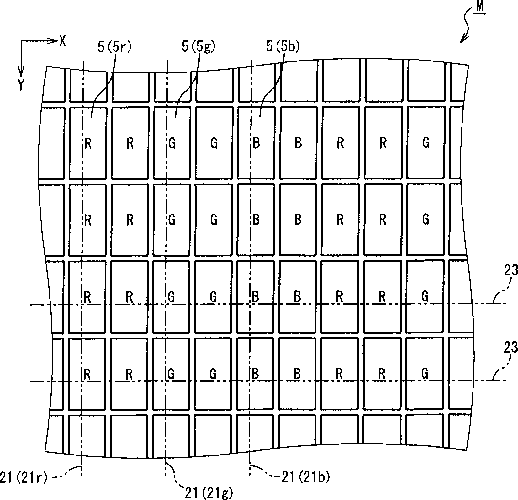
[0096] Here, a plurality of pixels 5 are set in the display device 1 . A plurality of pixels 5 are arranged in the X direction and the Y direction in the figure in the display area 7, and constitute a matrix M in which the X direction is the row direction and the Y direction is the column direction. In the display device 1 , a plurality of pixels 5 constitute a matrix M having m (m is an integer of 1 or greater) rows and 2×n (n is an integer of 1 or greater) columns. The display device 1 can display an image on the display surface 3 by selectively emitting light from the plurality of pixels 5 to the outside of the display device 1 via the display surface 3 . In addition, the display area 7 is an area where an image...


PUM


Abstract

An electro-optical device comprising a first substrate, a second substrate facing the first substrate, a light-emitting layer arranged between the first substrate and the second substrate which is capable of emitting light from a plurality of pixels including at least a first subpixel and a second subpixel, the first subpixel forming a first image and the second subpixel forming a second image, and a light-shielding layer arranged between the second substrate and the light-emitting layer having an opening which is capable of transmitting light emitted from a first subpixel in the light-emitting layer through the second substrate to a first range and transmitting light emitted from the second subpixel of the light-emitting layer through the second substrate to a second range.

Description

technical field [0001] The present invention relates to electro-optical devices and electronic equipment. Background technique [0002] Conventionally, an organic EL (Electro Luminescence) device is known as an electro-optical device. In addition, as an organic EL device, there is a display device capable of displaying a three-dimensional image by alternately shielding light from the organic EL element by a pair of left and right liquid crystal elements. (For example, refer to Patent Document 1). [0003] [Patent Document 1] Japanese Patent Laid-Open No. 2001-318341 [0004] Here, a structure in which different images are displayed in two directions in a display device including an organic EL element and a pair of liquid crystal elements will be described using cross-sectional views. Such as Figure 27 As shown in (a), this display device 600 has an organic EL element 601 and a pair of liquid crystal elements 603 . A pair of liquid crystal elements 603 are opposed to one...

Claims


Application Information

Patent Timeline
IPC IPC(8): H01L27/32
Inventor 野泽陵一
Owner 138东液晶显示器发展有限公司
Why Eureka
Try Eureka