Silica gel protected LED chip and manufacturing method thereof

A technology of light-emitting diodes and chips, applied in electrical components, circuits, semiconductor devices, etc., can solve problems such as silicone damage, affecting the efficiency of sorting, and affecting the appearance of chips, and achieve the effect of reducing viscosity and solving adhesion problems

Inactive Publication Date: 2009-07-22
LATTICE POWER (JIANGXI) CORP
View PDF0 Cites 5 Cited by
  • Summary
  • Abstract
  • Description
  • Claims
  • Application Information

AI Technical Summary

Problems solved by technology

After the silica gel is adhered to other workpieces, the silica gel will be damaged during the separation process, which will seriously affect the appearance of the chip. In addition, the adhesion phenomenon will also affect the sorting and packaging, and the chips will stick to each other during the sorting process. The phenomenon that the suction nozzle cannot be removed seriously affects the efficiency of sorting
The same problem exists in the automatic packaging process

Method used


Image

  • Silica gel protected LED chip and manufacturing method thereof
  • Silica gel protected LED chip and manufacturing method thereof

Examples


Embodiment 1

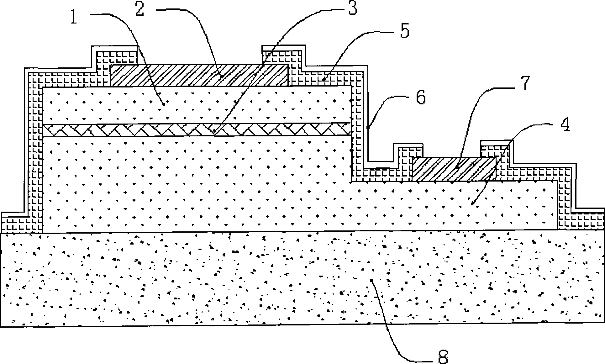
[0021] see figure 1 As shown, the chip structure is a horizontal structure. Substrate 8 is a growth substrate. The multilayer semiconductor structure on the substrate 8 is N-type layer 4, light-emitting layer 3 and P-type layer 2 from bottom to top, N-electrode 7 is arranged on N-type layer 4, and P-type electrode 2 is arranged on P-type layer , a silica gel layer 5 is formed on the surface of the multilayer semiconductor structure. The P electrode 4 and the N electrode 2 are exposed outside the silica gel layer for welding electrode leads. A film 6 for preventing the silicone layer from adhering to other workpieces is formed on the surface of the silicone layer 5 .

[0022] The production process of this embodiment is as follows:

[0023] First, a multi-layer semiconductor structure is formed on a growth substrate by MOCVD growth and chip technology, and a primary chip for further processing is made. Then apply glue on the chip at a speed of 500r / min for 10 seconds, bake...

Embodiment 2

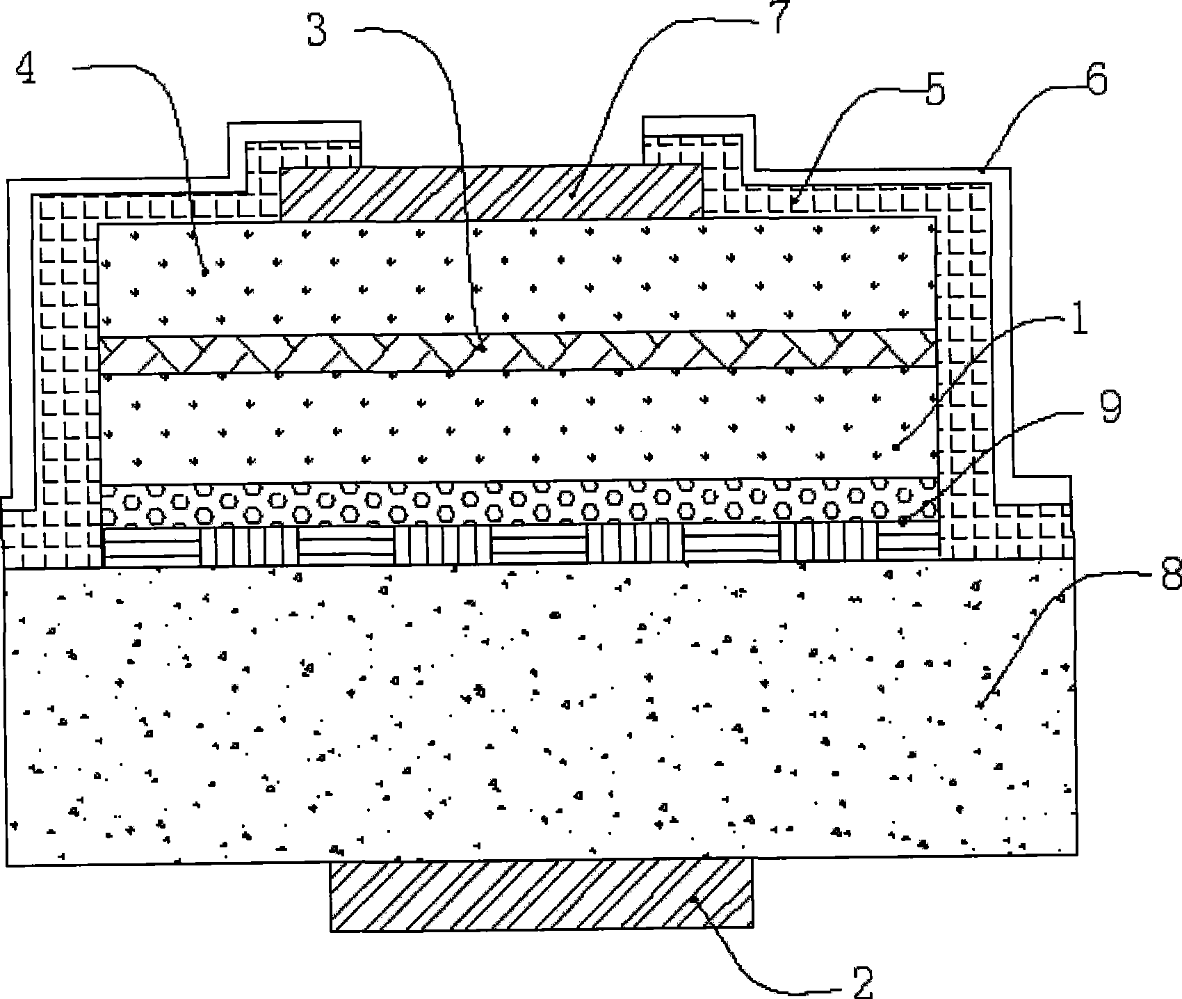
[0026] see figure 2 As shown, the chip structure is a vertical structure. The substrate 8 is a transfer substrate, and the structure is a flip-chip structure. Its structure from bottom to top is P electrode 2 , substrate 8 , transition layer 9 , P type layer 1 , light emitting layer 3 , N type layer 4 and N electrode 7 . A silica gel layer 5 is formed on the surface of the multilayer semiconductor structure. The N electrode 2 is exposed outside the silica gel layer for welding electrode leads. A film 6 for preventing the silicone layer from adhering to other workpieces is formed on the surface of the silicone layer 5 .

[0027] The production process of this embodiment is as follows:

[0028] First, through MOCVD growth and chip processing, such as figure 2 The primary chip shown is then glued on the primary chip at a speed of 3000r / min for 30 seconds, baked with a hot plate at 110°C for 120s, and masked with a photolithography plate at a rate of 1000mJ / cm 2 Expose to ...


PUM


Abstract

The invention discloses a light emitting diode (LED) chip protected by silica gel and a manufacture method thereof. The LED chip can avoid or reduce the occurrence of dice bonding and blockage of suction nozzles during production, thus improving the production efficiency. The LED chip comprises a substrate and a multilayer semiconductor structure formed on the substrate, wherein, a silica gel layer is formed on the surface of the multilayer semiconductor structure and a thin film used for preventing the silica gel layer from sticking to other workpieces is formed on the surface of the silica gel layer. The method put forward by the invention comprises the following steps: forming the multilayer semiconductor structure on a silicon substrate, forming a covered silica gel layer on the surface of the multilayer semiconductor structure and forming a layer of thin film used for preventing the silica gel layer from sticking to other workpieces on the surface of the silica gel layer. The method can effectively solve the sticking problem of the chip during dicing, film turning and sorting and packaging, etc.

Description

technical field [0001] The invention relates to a light emitting diode chip and a manufacturing method thereof. Background technique [0002] The preparation of GaN-based vertical light-emitting diodes by substrate lift-off method is the most commonly used method at present. This method requires bonding a substrate to the epitaxial wafer and then removing the substrate used for epitaxial growth. Defects such as gaps and bubbles often appear on the bonding surface, and the GaN epitaxial layer itself is thin and brittle, so it brings many difficulties to subsequent chip manufacturing, including scribing, sorting, flipping, and packaging. , Chips are often cracked or broken, which seriously affects the yield rate of chip manufacturing. Moreover, due to the material properties of GaN itself, cracks or fragments may appear in the process of sorting and packaging even if the chip is not prepared by lift-off technology, which also affects the yield rate of chip manufacturing. Wh...

Claims


Application Information

Patent Timeline
Patent Type & Authority Applications(China)
IPC IPC(8): H01L33/00
Inventor 刘军林章少华江风益王立
Owner LATTICE POWER (JIANGXI) CORP
Why Eureka
Try Eureka