Exposure method

An exposure method and exposure area technology, applied in the exposure field

Active Publication Date: 2009-07-29
UNITED MICROELECTRONICS CORP
View PDF0 Cites 15 Cited by
  • Summary
  • Abstract
  • Description
  • Claims
  • Application Information

AI Technical Summary

Problems solved by technology

However, traditional automatic feedback systems only provide a fixed feedback value for each wafer in each batch, which does not help the critical dimension variation between each exposure area on the wafer

Method used


Image

  • Exposure method
  • Exposure method
  • Exposure method

Examples


Embodiment Construction

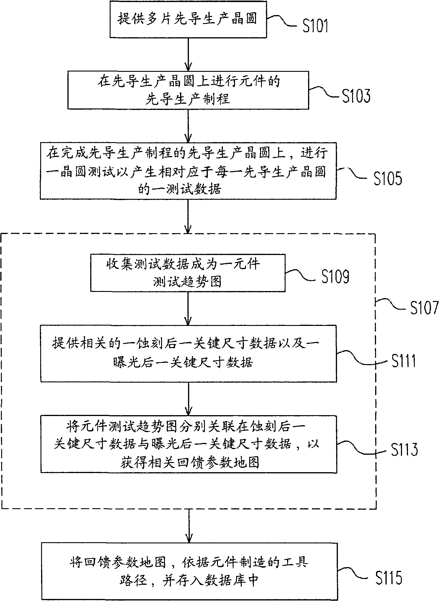
[0025] figure 1 Shown is a flow chart of a method for forming a feedback parameter map according to the present invention. Please refer to figure 1 , first provide a plurality of pilot production wafers (pilot-run wafer) in step S101. Wherein, the quantity of the pilot production wafers may be the quantity of a batch of wafers, for example, 25 wafers. Afterwards, in step S103 , a pilot run of a device is performed on each pilot wafer with a tool path. Among them, a component may be as small as a simple circuit component, or as large as a product with a complex circuit layout. In addition, the so-called toolpath refers to several kinds of process machines required to perform a series of process operations for producing the above-mentioned components, and the machines are sorted into a toolpath according to the sequence of process operations for producing the above-mentioned components. Afterwards, in step S105, a wafer test (wafer acceptable test, WAT) is performed on each ...


PUM


Abstract

The invention provides an exposure method which is used for preparing an element, comprising the steps as follows: a wafer with a plurality of exposure areas is provided; wherein, the wafer is covered by an photoresist layer; a feedback parameter map with a plurality of exposure area feedback parameter groups is provided; the exposure area feedback parameter groups are respectively corresponding to the exposure areas of the wafer; at least one group of exposure area feedback parameter group out of the exposure area feedback parameter groups is different from other exposure area feedback parameter groups; according to the feedback parameter map, an exposure preparation is carried out sequentially on each exposure area of the wafer by an exposure tool so as to pattern the photoresist layer on the wafer; wherein, when the exposure tool carries out the exposure preparation on each exposure area, the exposure preparation parameter group of the exposure tool is adjusted at the exposure area feedback parameter group corresponding to each exposure area according to the feedback parameter map.

Description

technical field [0001] The present invention relates to a method of exposure, and in particular to the ability to increase the shot-to-shot level of the exposure area on the same wafer during the wafer test (wafer acceptable test, WAT) step. An exposure method for the consistency of critical dimensions. Background technique [0002] In integrated circuit manufacturing, photolithography is used to transfer a custom circuit pattern on a photomask to a thin film formed on a wafer. The image transfer process includes forming a photoresist layer on an unprocessed layer, then using a photomask with a customized circuit pattern as a mask to irradiate the photoresist layer, followed by a step of developing the photoresist layer, and then, Using the patterned photoresist layer as a mask, an etching step is performed to etch the untreated layer to complete the image transfer process. [0003] Generally speaking, the basic parameter affecting the critical dimension (CD) of the photol...

Claims


Application Information

Patent Timeline
Patent Type & Authority Applications(China)
IPC IPC(8): G03F7/20H01L21/027
Inventor 陈儒德吴文宗
Owner UNITED MICROELECTRONICS CORP
Why Eureka
Try Eureka