Etching method, etching apparatus, computer program and storage medium

A technology of etching and etching gas, which is applied in the direction of discharge tubes, electrical components, semiconductor/solid-state device manufacturing, etc., to achieve excellent effects

Inactive Publication Date: 2009-08-12
TOKYO ELECTRON LTD
View PDF4 Cites 7 Cited by
  • Summary
  • Abstract
  • Description
  • Claims
  • Application Information

AI Technical Summary

Problems solved by technology

[0016] Here, when etching a tungsten film formed by buried CVD (blanket CVD), as disclosed in paragraphs (0040) to (0042) of JP-A-7-226393, it is proposed that the The frequency of the bias power is switched from 13.56MHz to 800kHz, or from 800kHz to 13.56MHz, but if the etching target film is a thin film of Low-k material different from the tungsten film, the above technology cannot be directly applied

Method used


Image

  • Etching method, etching apparatus, computer program and storage medium
  • Etching method, etching apparatus, computer program and storage medium
  • Etching method, etching apparatus, computer program and storage medium

Examples


Embodiment Construction

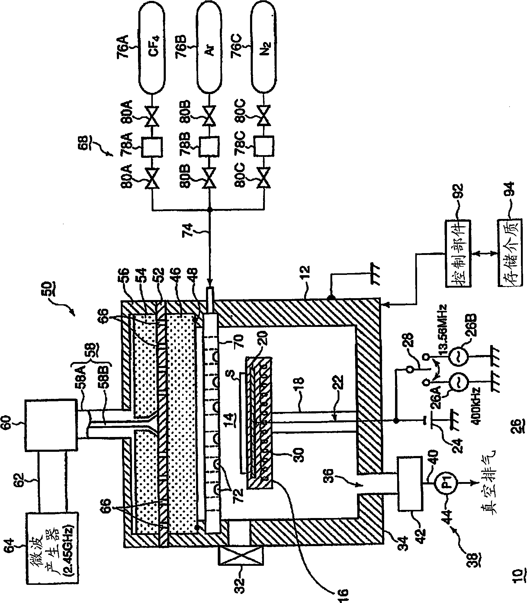
[0046] Hereinafter, an embodiment of an etching method, an etching apparatus, a computer program, and a recording medium of the present invention will be described with reference to the drawings.

[0047] figure 1 It is a configuration diagram showing an example of the etching apparatus of the present invention. As shown in the figure, for example, the side wall and the bottom of the etching device 10 are made of conductors such as aluminum, and have a cylindrical processing container 12 formed as a whole. The inside of the etching device 10 is constituted as a closed processing space 14. Plasma is formed in the processing space 14 . The processing vessel 12 itself is grounded.

[0048] In the processing container 12 is accommodated a disc-shaped mounting table 16 on which an object to be processed, for example, a semiconductor wafer S is mounted on the upper surface. The mounting table 16 is formed in a flat substantially disc shape from ceramics such as alumina as a heat...


PUM


Abstract

An etching method for etching an etching object film having a dielectric constant smaller than that of the SiO2 film formed on the object (S) to be processed. The method comprises a step of mounting the object (S) on a susceptor (16) in an evacuatable processing vessel (12), a step of supplying a predetermined etching gas into the processing vessel (12) and converting the etching gas into plasma, and a step of applying high-frequency power of a predetermined frequency as bias power to the susceptor (16) in the presence of the etching gas plasma. The step of applying the high-frequency power as bias power includes a first sub-step of applying high-frequency power of a first frequency as bias power and a second sub-step of applying high-frequency power of a second frequency different from the first one as a bias power.

Description

technical field [0001] The present invention claims priority to Japanese Patent Application No. 2006-228989 filed on August 25, 2006, and makes the present invention with reference to the entire contents of Japanese Patent Application No. 2006-228989. [0002] The present invention relates to an etching method and an etching device, in particular to an etching method and an etching device for forming holes (holes) such as via holes and via holes and grooves (grooves) on the surface of a target object such as a semiconductor wafer. In addition, the present invention also relates to a computer program for causing an etching device to execute an etching method, and a recording medium storing the computer program. Background technique [0003] Usually, in order to manufacture semiconductor devices, various processes such as film formation and pattern etching are repeated on semiconductor wafers to manufacture desired devices. The line width and hole (hole) diameter are further ...

Claims


Application Information

Patent Timeline
Patent Type & Authority Applications(China)
IPC IPC(8): H01L21/3065H01L21/768
CPCH01L21/76802H01J37/32165H01J37/32192H01L21/31116H01L21/3065
Inventor 西塚哲也
Owner TOKYO ELECTRON LTD
Why Eureka
Try Eureka