Raw gas supply system, and filming apparatus

A raw material gas and supply system technology, applied in the direction of electrical components, thin material handling, transportation and packaging, etc., can solve the problem of unable to supply raw material gas, etc., to suppress the generation of particles, maintain reproducibility, and suppress resolidification or reliquefaction Effect

Inactive Publication Date: 2010-07-07
TOKYO ELECTRON LTD
View PDF3 Cites 4 Cited by
  • Summary
  • Abstract
  • Description
  • Claims
  • Application Information

AI Technical Summary

Problems solved by technology

Therefore, a sufficient amount of source gas cannot be supplied into the processing container

Method used


Image

  • Raw gas supply system, and filming apparatus
  • Raw gas supply system, and filming apparatus
  • Raw gas supply system, and filming apparatus

Examples


Embodiment Construction

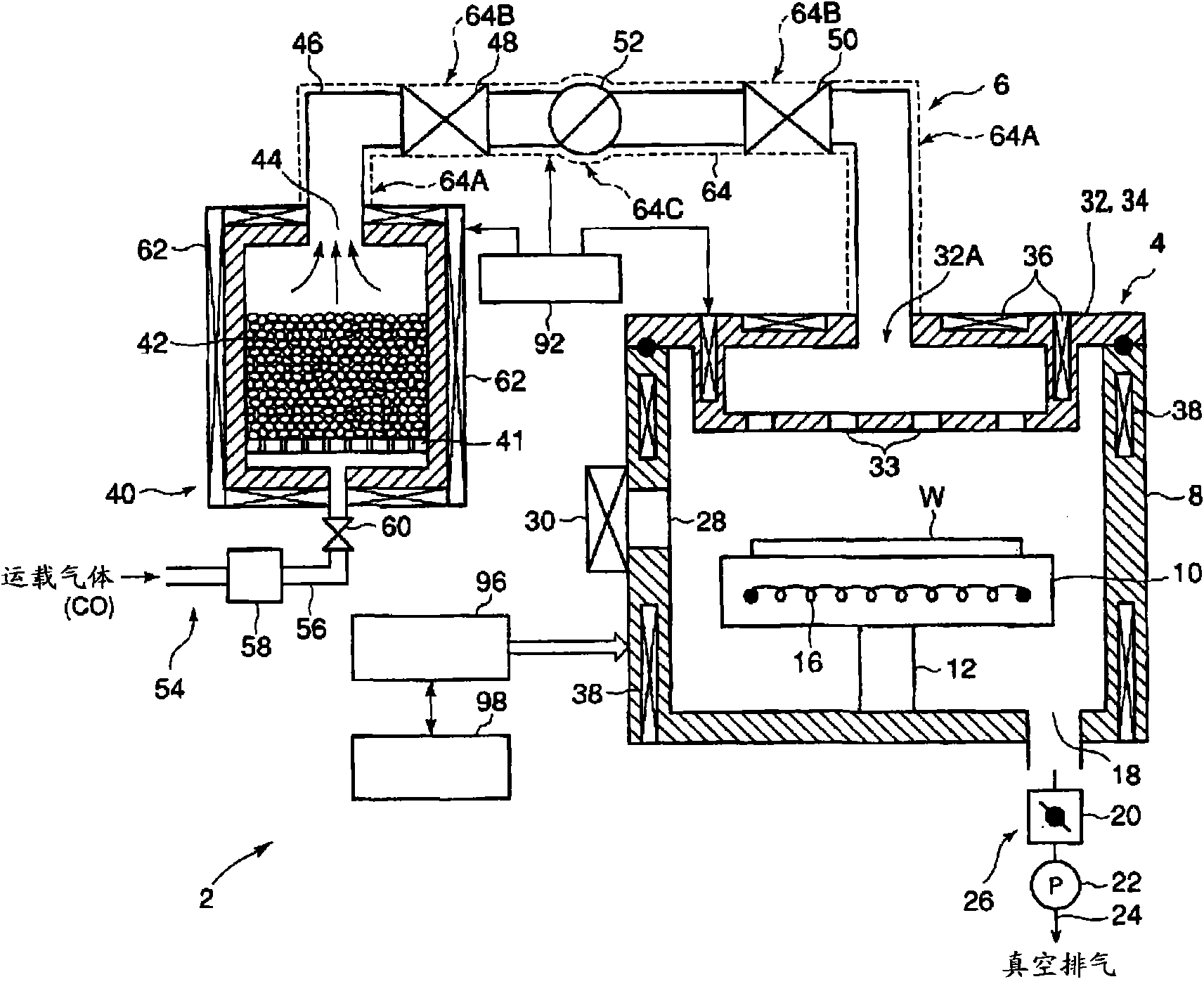
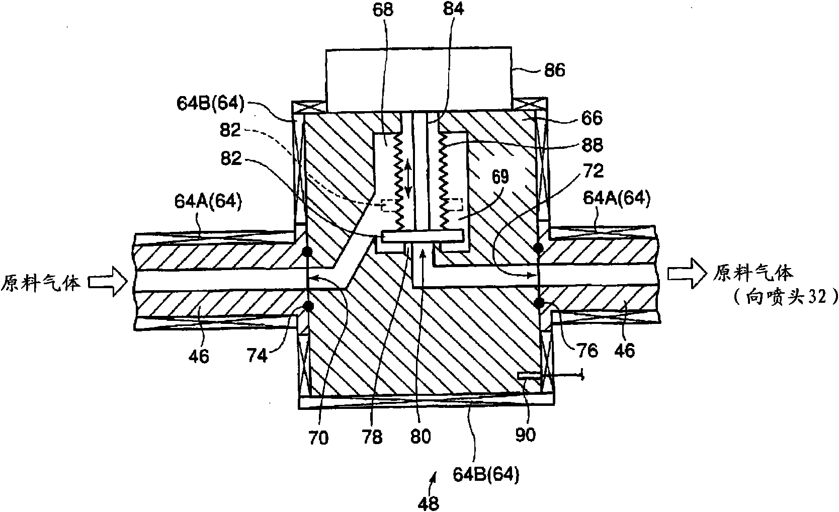
[0027] Hereinafter, preferred embodiments of a source gas supply system and a film forming apparatus according to the present invention will be described with reference to the drawings. figure 1 is a schematic configuration diagram showing a film forming apparatus having a source gas supply system. figure 2 It is a cross-sectional configuration diagram showing an example of an on-off valve used in a raw material gas supply system. In the embodiments described below, for Ru 3 (CO) 12 An example of forming a Ru metal film on a semiconductor wafer W as an object to be processed will be described using CO (carbon monoxide) as a carrier gas as a solid raw material.

[0028] Such as figure 1 As shown, the film forming apparatus 2 of the present embodiment has, as main constituent elements, a film forming apparatus main body 4 as a gas use system for actually performing a film forming process on a semiconductor wafer W as an object to be processed; A raw material gas supply syst...


PUM


Abstract

Provided is a raw gas supply system (6) for supplying a raw gas to a gas using system (2) set in a pressure-reduced atmosphere. The system comprises a material tank (40) for reserving a liquid material or a solid material, a material passage (46) connected at its one end to the material tank and at its other end to the gas using system, a carrier gas supply mechanism (54) for supplying a carrier gas to the inside of the material tank, ON / OFF valves (48 and 50) disposed midway of the material passage, a heater (64) for heating the material passage and the ON / OFF valves, and a temperature control unit (92) for controlling the heater. The material passage and the ON / OFF valves are formed of a metal material having an excellent heat conductivity.

Description

technical field [0001] The present invention relates to a film forming device for forming a thin film on the surface of a target object such as a semiconductor wafer, and a supply system for supplying a raw material gas thereto, and particularly relates to a device for supplying a useful semiconductor device by vaporizing a raw material with a low vapor pressure and not easily evaporated. Supply system of raw material gas and film forming device. Background technique [0002] Generally, when manufacturing a semiconductor device, in order to manufacture a desired device, various processes such as film formation and pattern etching are repeatedly performed on a semiconductor wafer. Nowadays, in accordance with the demands for higher integration and high miniaturization of semiconductor devices, both the line width and aperture are becoming finer. For wiring materials and embedding materials, it is necessary to further reduce the resistance due to the miniaturization of variou...

Claims


Application Information

Patent Timeline
Patent Type & Authority Applications(China)
IPC IPC(8): C23C16/448H01L21/31
CPCC23C16/4481Y10T137/8376Y10T137/8158
Inventor 原正道五味淳前川伸次山本薰多贺敏
Owner TOKYO ELECTRON LTD
Why Eureka
Try Eureka