Supercharge Your Innovation With Domain-Expert AI Agents!

Semiconductor sheets and methods for fabricating the same

A semiconductor and sheet technology, applied in the field of semiconductor sheets and their preparation, can solve problems such as solar power system limitations and cost increases

Inactive Publication Date: 2009-08-19
MOTECH AMERICAS
View PDF2 Cites 2 Cited by
  • Summary
  • Abstract
  • Description
  • Claims
  • Application Information

AI Technical Summary

Problems solved by technology

Since the cost of silicon raw material increases with the improvement of the purity of silicon raw material, the application of solar power system will be limited by the cost of silicon

Method used


Image

  • Semiconductor sheets and methods for fabricating the same
  • Semiconductor sheets and methods for fabricating the same
  • Semiconductor sheets and methods for fabricating the same

Examples


Embodiment Construction

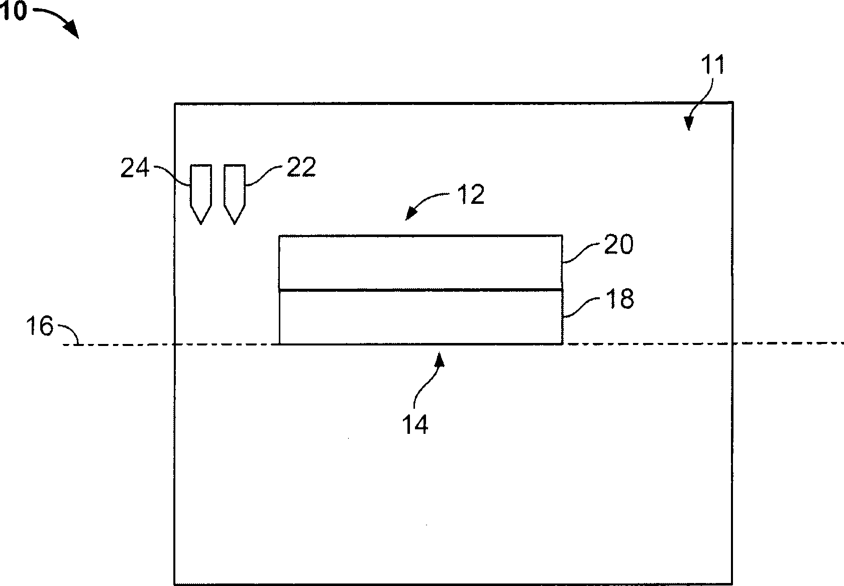
[0012] Silicon is currently one of the most commonly used semiconductor materials, also known as raw materials, for the preparation of semiconductor wafers. Accordingly, the terms "semiconductor" and "semiconductor material" as used in the present invention refer to silicon-based components and silicon materials. However, as those skilled in the art will readily recognize, other semiconductor materials other than silicon and / or including non-silicon materials can also be prepared using the apparatus and methods of the present invention. Also, although only the use of silicon powder raw material for making silicon flakes is described here, silicon raw material sheets may be used without departing from the invention.

[0013] figure 1 is available for the preparation of silicon flakes (not in figure 1 A schematic diagram of an exemplary embodiment of the furnace apparatus 10 shown in ). The furnace facility 10 includes a controlled atmosphere 11 in order to prevent inert subs...


PUM


Abstract

A sheet of semiconductor material (28) is provided, including a lower surface and an upper surface. The sheet of semiconductor material is fabricated by a process including forming a first layer (32) of silicon powder (34) that has a lower surface (36) and an opposite upper surface (38), depositing a second layer (40) across the upper surface of the first layer, wherein the second layer of silicon powder (42) has a lower surface (44) and an opposite upper surface (46) and has a substantially similar melting point to the first layer of silicon powder, and heating at least one of the first and second layers of silicon powder to initiate a controlled melt of one of the first and second layer of silicon powder and to initiate crystallization (43) of at least one of the first and second layers of silicon powder.

Description

[0001] Statement Regarding Federally Funded Research and Development [0002] Pursuant to Contract No. 70NANBB3H3061, the United States Government may have rights in this invention. technical field [0003] The field of the invention relates generally to semiconductor wafers, and more specifically to semiconductor wafers and methods for their preparation. Background technique [0004] Cutting thin sheets of semiconductor material into wafers of predetermined dimensions is well known. Wafers formed from semiconductor materials can be used for a variety of purposes. For example, at least some known solar power systems employ semiconductor substrates, typically fabricated from silicon. The use of solar power systems has grown dramatically over the past decade, and therefore, the demand for semiconductor wafers has also grown over the past decade. Although the expression "solar power" is used herein, those skilled in the art will recognize that the discussion applies to a var...

Claims


Application Information

Patent Timeline
Patent Type & Authority Applications(China)
IPC IPC(8): C30B1/00C30B28/02C30B29/06
CPCH01L31/1872H01L31/1804Y02E10/50Y02E10/547Y10T428/12028Y02P70/50
Inventor R·容奇克
Owner MOTECH AMERICAS
Features
  • R&D
  • Intellectual Property
  • Life Sciences
  • Materials
  • Tech Scout
  • Unparalleled Data Quality
  • Higher Quality Content
  • 60% Fewer Hallucinations
Learn More