Built-in self-test method of FPGA logical resource

A technology of built-in self-test and logic resources, applied in the field of built-in self-test based on scan register FPGA logic resources, it can solve the problem of lack of in-depth introduction, and achieve the goal of simplifying the retrieval method, simplifying the configuration structure, and improving the test efficiency. Effect

Active Publication Date: 2009-08-26
BEIJING MXTRONICS CORP +1
View PDF0 Cites 24 Cited by
  • Summary
  • Abstract
  • Description
  • Claims
  • Application Information

AI Technical Summary

Problems solved by technology

However, the article only briefly introduces the basic structure of FPGA logic BIST, and gives the general and common steps of BIST test structure, but does not make a further in-depth introduction to the method

Method used


Image

  • Built-in self-test method of FPGA logical resource
  • Built-in self-test method of FPGA logical resource
  • Built-in self-test method of FPGA logical resource

Examples


Embodiment Construction

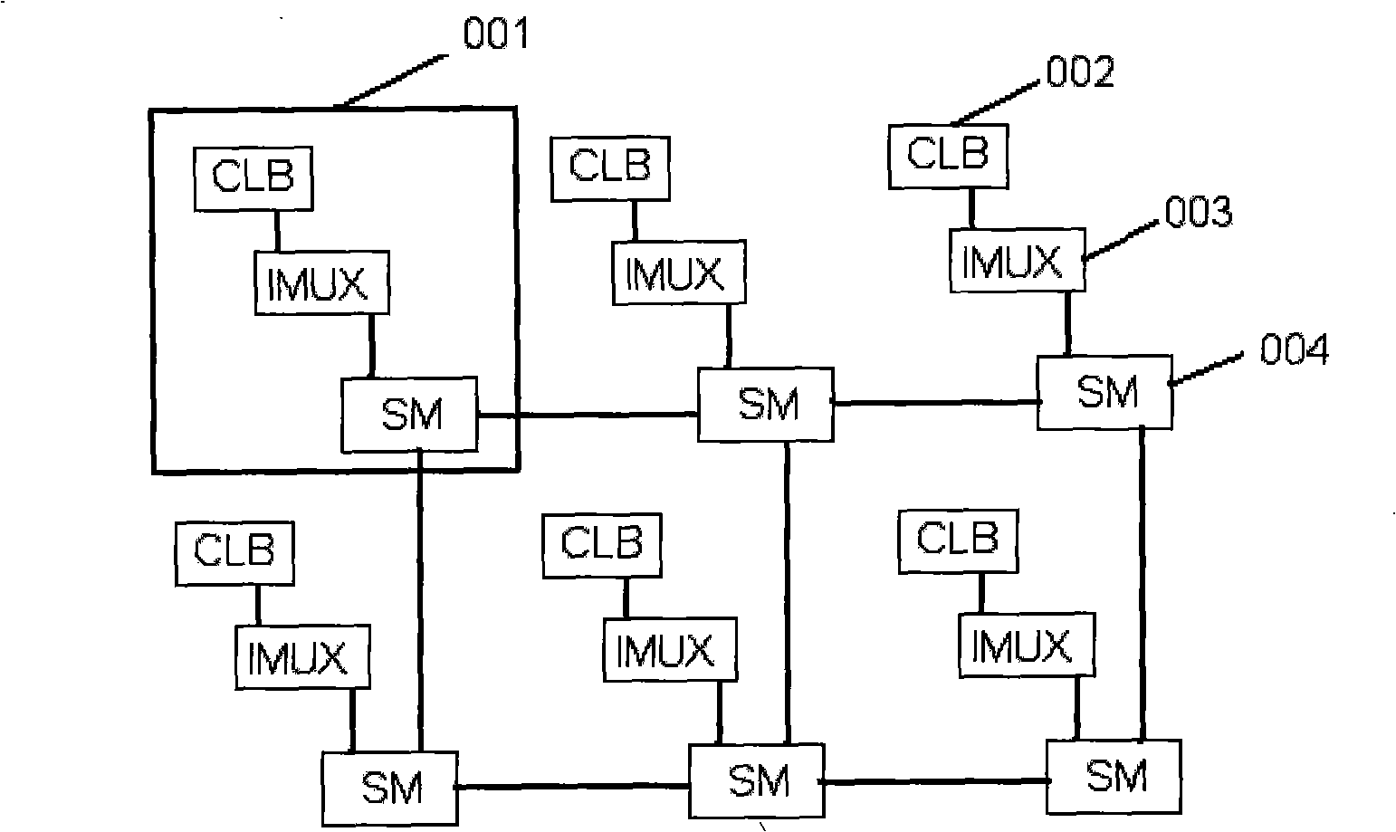
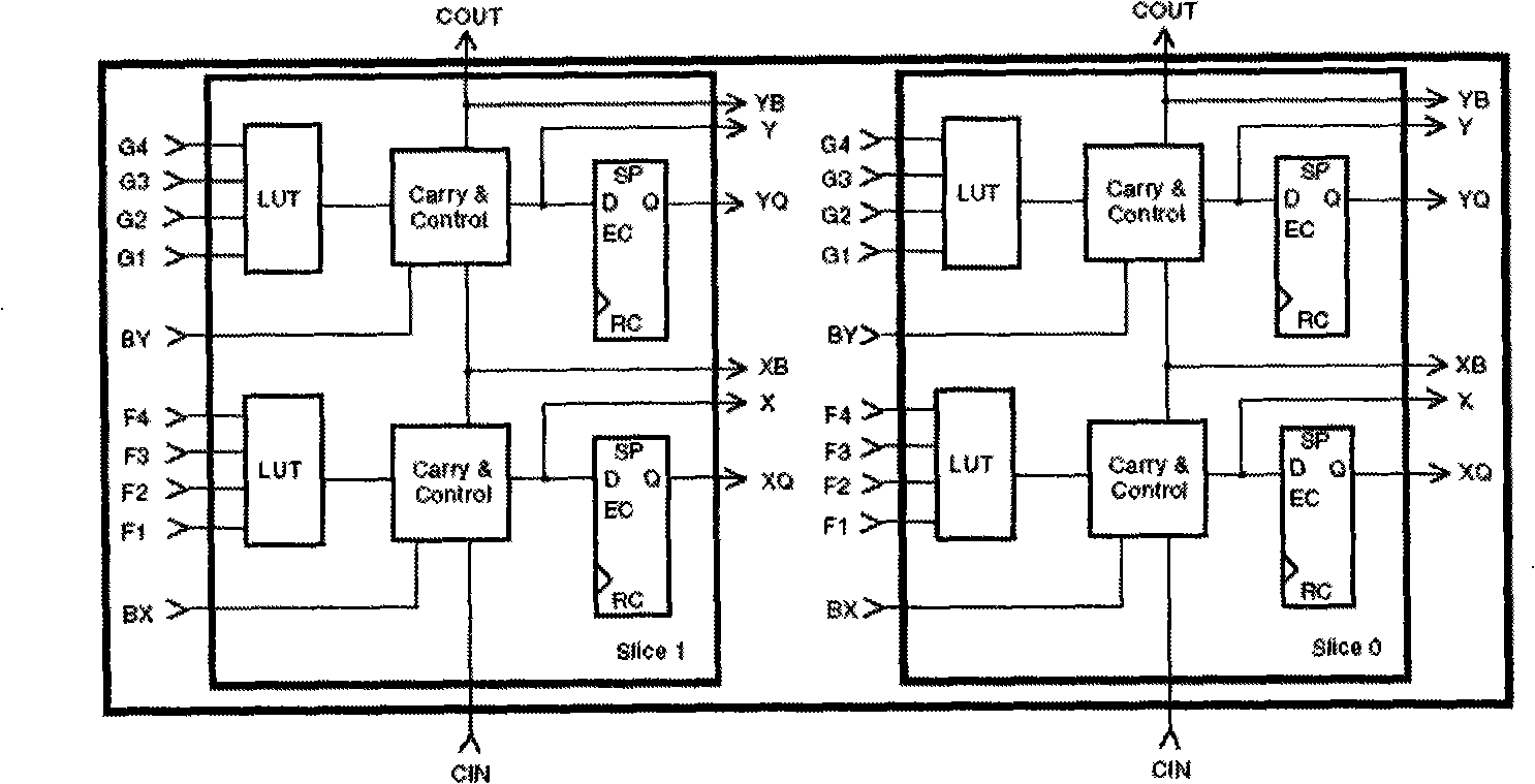
[0030] FPGA basic circuit structure such as figure 1 As shown, it is mainly composed of TITLE array 001 and input and output module 005. Programmable logic module 002 is a logic unit in one of TITLE array 001, and it realizes interconnection with surrounding programmable logic modules through IMUX003 and switch matrix 004 , users can flexibly implement various functions by configuring the programmable logic module 002. The configurable logic module 002 is the logical unit in the TITLE array 001, such as figure 2 The configurable logic module 002 shown is mainly composed of two identical SLICE units. It realizes the interconnection with the surrounding programmable logic modules through the IMUX003 and the switch matrix 004, and the user can flexibly realize it by configuring the configurable logic module 002 various functions.

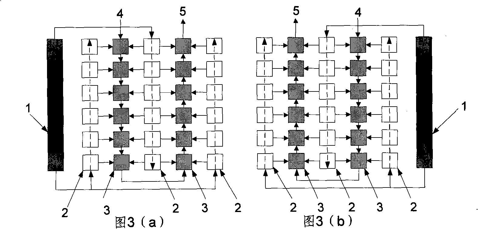
[0031] The built-in self-test structure of the present invention is as image 3 As shown, the built-in self-test process is as follows:

[0032] ...


PUM


Abstract

The invention provides a built-in self-test method of FPGA logical resource. The internal logical module of FPGA is alternately divided into a left half part and a right half part according to row. In the test process, the logical module array of the right half part is firstly configured as a to-be-tested circuit, and the rest logical module arrays are configured as a test vector generating circuit and an output response analyzing circuit, and then the logical module array of the left half part is configured as the to-be-tested circuit, and the rest logical module arrays are configured as the test vector generating circuit and the output response analyzing circuit. The circuit structure is not changed in each process. The logical resource is covered by multiple configurations and the test result is output by a built-in scan register chain. All configurations in the invention are as follows: all logical modules configured as the response analyzing circuits are in cascade connection end to end according to one-dimensional array, so as to simplify the self-test result retrieval manner. Provided that the test coverage is 100%, the built-in self-test method reduces times of the configurations of FPGA logical resource, reduces test cost and increases test flexibility, so as to improve test efficiency.

Description

technical field [0001] The invention relates to a testing method of an FPGA chip, in particular to a built-in self-testing method based on scanning register FPGA logic resources. Background technique [0002] FPGA testing takes advantage of its reprogrammable feature to cover all resources under test through multiple configurations. There are mainly two methods for testing it: external testing and built-in self-testing. During external testing, the FPGA device is configured as a corresponding testing circuit, and external equipment is used to apply test vectors and special equipment to analyze the output results. This method occupies a large number of pins, resulting in The test depends on the package; compared with the external test, the vector application and response analysis of the built-in self-test method are completed internally, without the need for special test equipment and a large number of pins, which reduces the test cost and increases the test flexibility. [...

Claims


Application Information

Patent Timeline
Patent Type & Authority Applications(China)
IPC IPC(8): G01R31/3185
Inventor 张志权文治平陈雷王慜张帆周涛
Owner BEIJING MXTRONICS CORP
Why Eureka
Try Eureka