Method for increasing test coverage of scan chain and device thereof

A test coverage and scan chain technology, applied in static memory, instruments, etc., can solve the problems of reducing logic coverage and low chip test coverage, to improve overall test coverage, achieve testability, and improve logic testing. The effect of coverage

Active Publication Date: 2009-08-26
BEIJING VIMICRO ARTIFICIAL INTELLIGENCE CHIP TECH CO LTD
View PDF6 Cites 16 Cited by
  • Summary
  • Abstract
  • Description
  • Claims
  • Application Information

AI Technical Summary

Problems solved by technology

[0010] The purpose of the present invention is to provide a method and device for improving scan chain test coverage, to solve the problem of reducing the logic coverage of the test due to the inability to complete the capture function in the capture mode in the prior art, resulting in low overall test coverage of the chip The problem

Method used


Image

  • Method for increasing test coverage of scan chain and device thereof
  • Method for increasing test coverage of scan chain and device thereof

Examples


Embodiment Construction

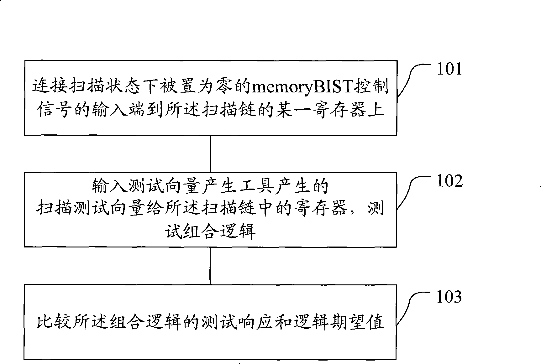
[0029] In order to make the above objects, features and advantages of the present invention more comprehensible, the present invention will be further described in detail below in conjunction with the accompanying drawings and specific embodiments.

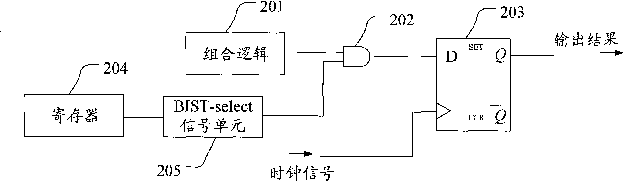
[0030] The solution provided by the present invention improves the logic test coverage of the chip by improving the control logic of the built-in self-test (BIST) of the memory (memory) during the scan chain test, thereby improving the overall test coverage of the chip.

[0031] The embodiment of the present invention relates to a chip designed to improve scan chain test coverage. In the chip design, many memories are used, including registfile, 6T-sram, and oneT-sram.

[0032] When performing the scan chain test, it was found that the test coverage rate of the memory BIST logic was very low, only about 40%. After testing, it is found that it is because a lot of memory is used in the above-mentioned chip design, and these memories...


PUM


Abstract

The invention provides a method for increasing the test coverage of a scan chain and a device thereof; wherein, the method for increasing the test coverage of the scan chain comprises: an input end of built-in self testing control signals of a memory being set to be zero in a scanning mode is connected into one register in the scan chain; scan test vector generated by a test vector generation tool is input into the scan chain comprising the register to test combinational logic; the test response and logic expected value of the combinational logic are compared. The method for increasing the test coverage of the scan chain provided by the invention causes that the built-in self testing control signals of the memory can be controlled when the scan chain tests, and realizes the testability of the built-in self testing logic of the memory in the scan mode, thus increasing the logic test coverage of the scan chain test and further increasing the whole test coverage of a chip.

Description

technical field [0001] The invention relates to the technical field of memory testing, in particular to a method and a device for improving scan chain test coverage. Background technique [0002] In order to ensure the correctness of manufactured products, integrated circuits need to use test vectors (test patterns) to test whether there are manufacturing defects. The so-called test vector is the test stimulus loaded to the integrated circuit chip during the test. The test patterns are mainly divided into: a test pattern (ROMBIST Pattern) for testing the read-only memory in the chip, a test pattern (RAM BIST Pattern) for testing the random access device in the chip, and a scan chain test pattern (Scan Pattern). [0003] Wherein, the scan chain is composed of multiple registers, and the stored values ​​in the multiple registers are controlled by an automatic test pattern generation tool (Auto Test Pattern Generation, ATPG), so as to form a scan chain test vector. [0004] S...

Claims


Application Information

Patent Timeline
Patent Type & Authority Applications(China)
IPC IPC(8): G11C29/14
Inventor 张浩
Owner BEIJING VIMICRO ARTIFICIAL INTELLIGENCE CHIP TECH CO LTD
Why Eureka
Try Eureka