Method for growing high-quality indium nitride single crystal epitaxial film

A technology of indium nitride single crystal and epitaxial film, applied in gaseous chemical plating, metal material coating process, coating, etc., can solve the difficulty of InN single crystal epitaxial film, low ammonia cracking efficiency, low decomposition temperature, etc. question

Inactive Publication Date: 2009-09-09
INST OF SEMICONDUCTORS - CHINESE ACAD OF SCI
View PDF0 Cites 3 Cited by
  • Summary
  • Abstract
  • Description
  • Claims
  • Application Information

AI Technical Summary

Problems solved by technology

However, due to the relatively high requirement of the N equilibrium gas pressure on the surface during the growth process of InN, the decomposition temperature of InN is relatively low, which determines that InN can only grow at a lower growth temperature.
The MOCVD growth of InN uses ammonia gas as the N source. At a relatively low growth temperature (~500°C), the cracking efficiency of ammonia gas is very low, and the surface lacks reactive N atoms. The growth of

Method used


Image

  • Method for growing high-quality indium nitride single crystal epitaxial film
  • Method for growing high-quality indium nitride single crystal epitaxial film
  • Method for growing high-quality indium nitride single crystal epitaxial film

Examples


Embodiment Construction

[0018] In order to make the object, technical solution and advantages of the present invention clearer, the present invention will be described in further detail below in conjunction with specific embodiments and with reference to the accompanying drawings.

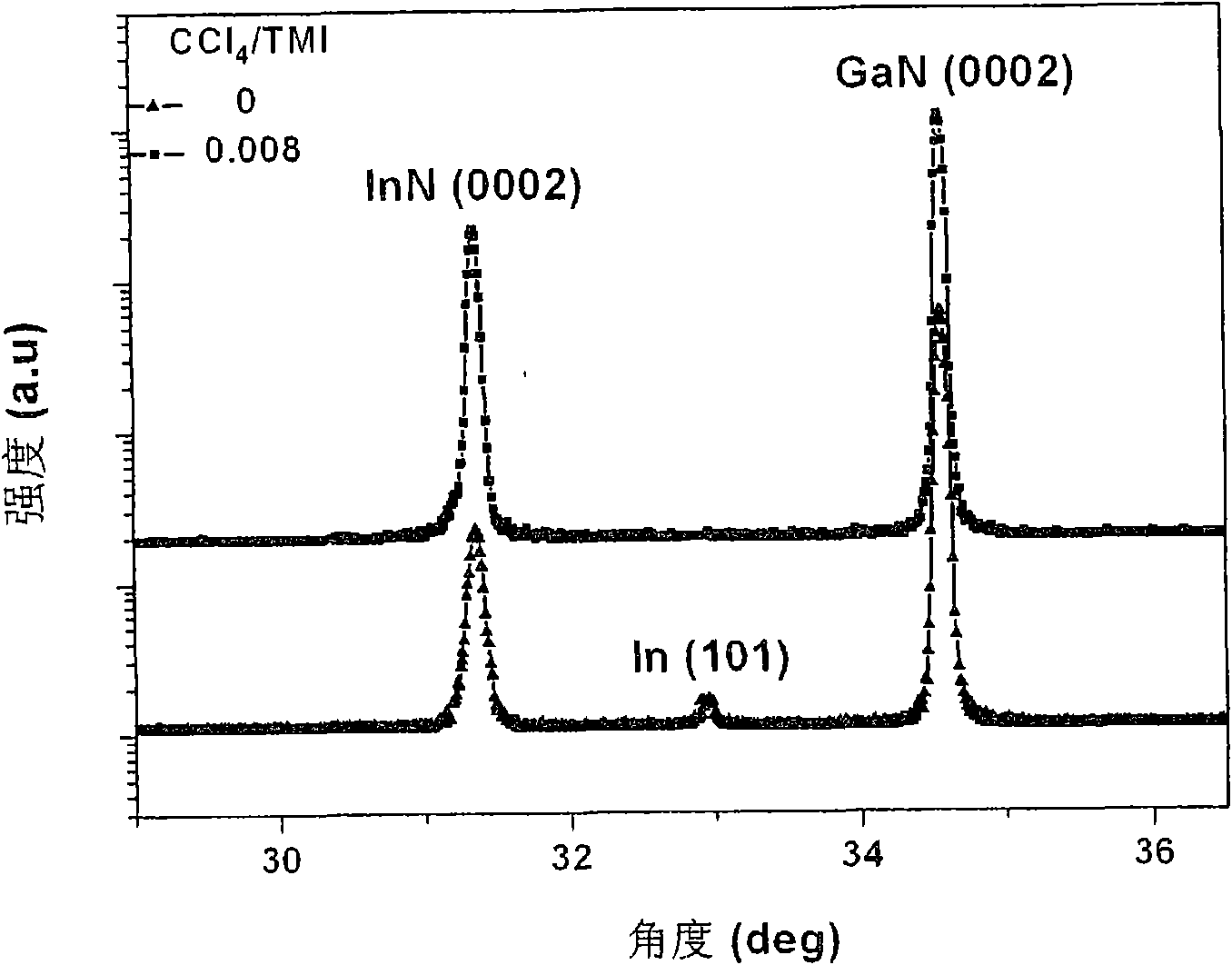
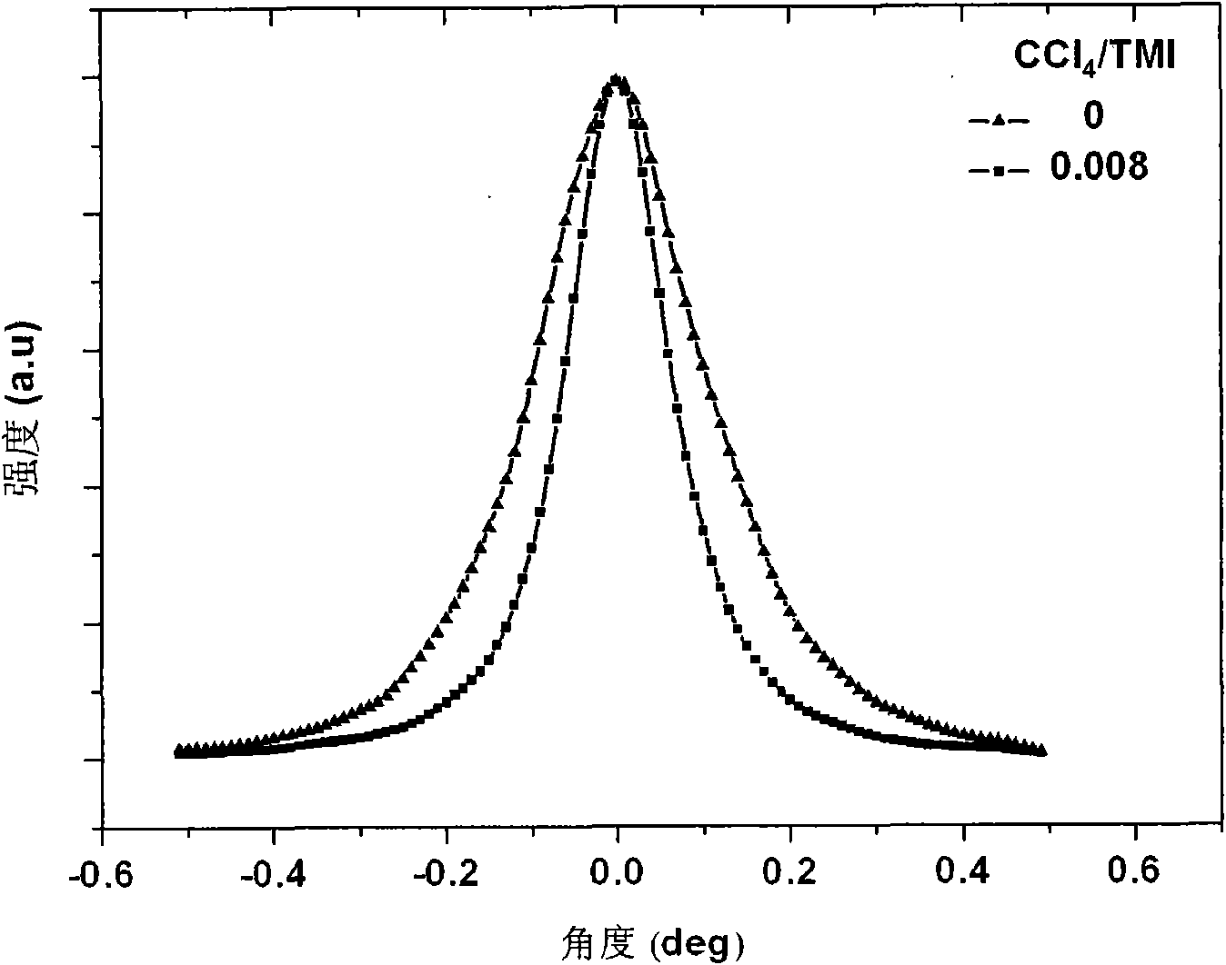
[0019] The key of the invention is to solve the problem of relatively poor crystal quality during the InN heteroepitaxial growth process. Since the decomposition temperature of InN is very low, the growth can only be carried out at a lower temperature, and the cracking efficiency of ammonia gas is very low when MOCVD epitaxy grows InN at a lower growth temperature, and the surface lacks reactive N atoms. Indium drops often appear in the grown InN epitaxial film, and the migration ability of surface adatoms is relatively low, making the InN single crystal epitaxial growth very difficult. In order to solve the problems of indium drops and low surface migration ability during InN epitaxy, the present invention proposes to in...


PUM


Abstract

The invention provides a method for growing a high-quality indium nitride single crystal epitaxial film, which is to introduce small amount of halide while growing indium nitride, and comprises the following steps: selecting a substrate; placing the substrate in a metal-organic chemical vapor deposition system, raising the temperature, and introducing ammonia gas for pretreatment; and reducing temperature to a growth temperature, and simultaneously introducing trimethylindium (TMI), the ammonia gas (NH3) and the small amount of the halide to grow the high-quality indium nitride single crystal epitaxial film. The method can improve the crystallization quality of InN and the surface smoothness.

Description

technical field [0001] The invention relates to the technical field of semiconductors, in particular to an epitaxial growth method of a high-quality indium nitride single crystal epitaxial film. Background technique [0002] Group III nitride semiconductor indium nitride (InN) has received more and more attention and research due to its unique physical and chemical properties. In Group III nitrides, InN has the smallest effective mass and theoretically has the highest carrier mobility, so it has broad application prospects in the field of high-speed devices; InN has the smallest direct bandgap, making it an infrared Suitable materials for wavelength light-emitting devices. However, due to the difficulty in the preparation of bulk single crystals of InN, there is no relevant report on the preparation of bulk single crystals. However, the preparation of InN single crystal epitaxial film becomes difficult because of the low decomposition temperature of InN and the lack of mat...

Claims


Application Information

Patent Timeline
IPC IPC(8): C23C16/34C23C16/52
Inventor 王莉莉张书明杨辉梁骏吾
Owner INST OF SEMICONDUCTORS - CHINESE ACAD OF SCI
Why Eureka
Try Eureka