

Boundary scanning chip failure detection device and method
A fault detection and boundary scan technology, applied in measurement devices, measurement of electricity, measurement of electrical variables, etc., can solve the problems of inaccurate fault location and difficult detection, and achieve the effect of improving work efficiency
- Summary
- Abstract
- Description
- Claims
- Application Information
AI Technical Summary
Problems solved by technology
Method used
Image

Examples
Embodiment Construction
[0028] Embodiments of the present invention will be described in detail below in conjunction with the accompanying drawings.
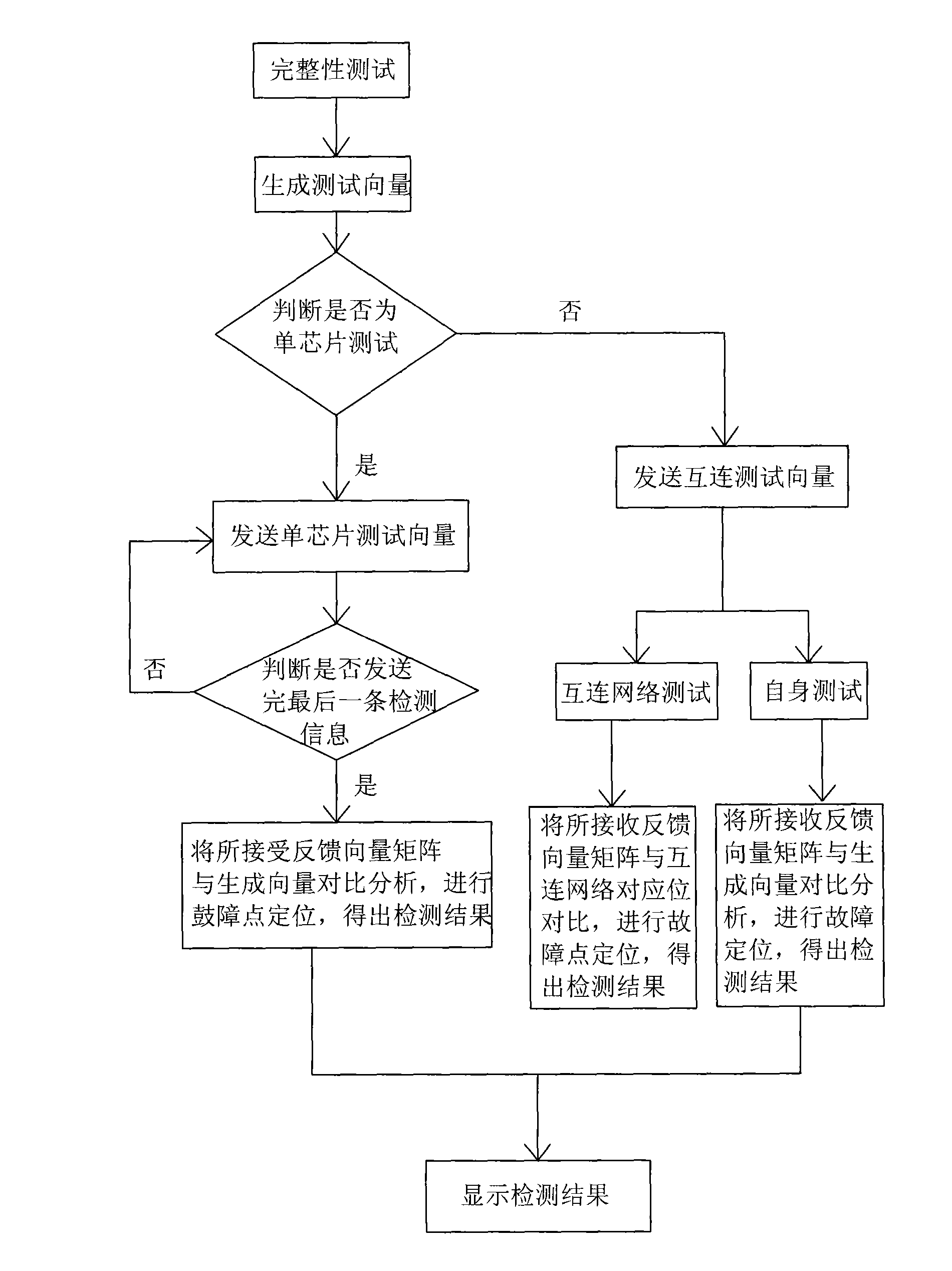
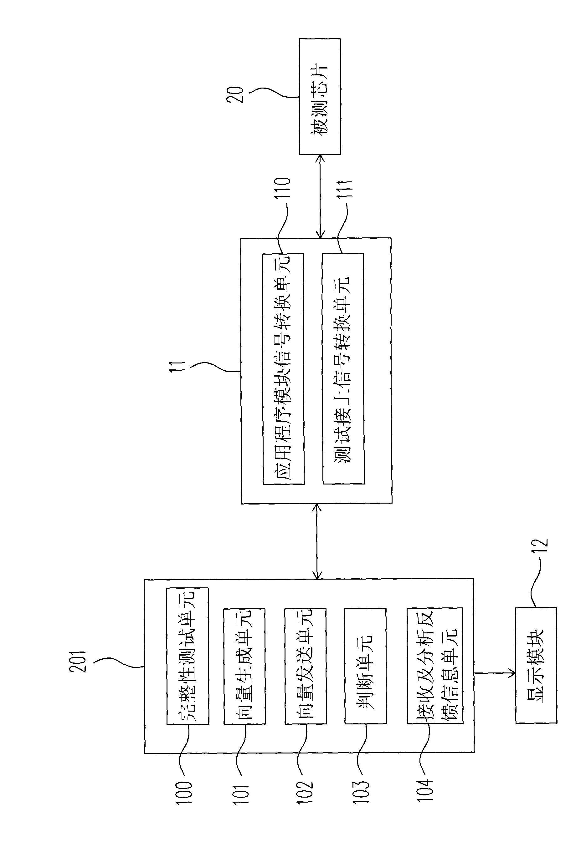
[0029] The function realization of the present invention mainly controls the resident program in the microprocessor on the JTAG (Joint TextAction Group) conversion module to complete the reading and writing of the test vector through the user operation application program, and the microprocessor generates the JTAG test interface drive signal to drive the JTAG bus , and finally the application program analyzes and diagnoses the test results and uses relevant information files to locate the fault point.
[0030] figure 1 It is a schematic flow chart of the boundary scan chip fault detection method of the present invention. As shown in the figure, a boundary scan chip fault detection method uses an application program to connect to the test interface of the chip under test 20 to perform comprehensive detection on the chip under test 20;
[0031] The conc...
PUM
 Abstract
Description
Claims
Application Information