Active component array substrate and LCD panel
A liquid crystal display panel and active component technology, applied in electrical components, electric solid state devices, semiconductor devices, etc., can solve problems such as cross shadow and display screen flicker, achieve large storage capacitance, increase aperture ratio, and improve the effect of display quality
Inactive Publication Date: 2011-01-05
CPT TECH GRP +1
View PDF0 Cites 0 Cited by
- Summary
- Abstract
- Description
- Claims
- Application Information
AI Technical Summary
Problems solved by technology
Method used
View moreImage
Smart ImageViewing Examples

Examples
no. 1 example
no. 2 example
no. 3 example
Login to View More PUM
 Abstract
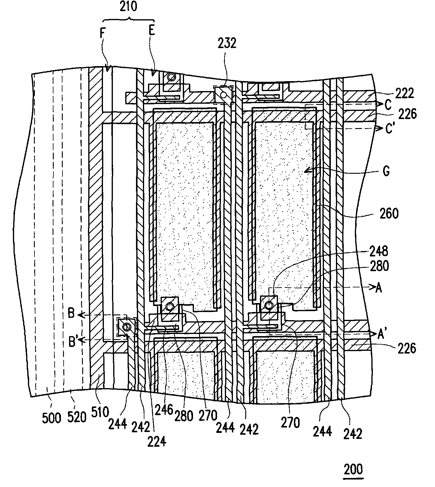
The invention is applicable to the technical field of LCD, and provides an active component array substrate comprising a substrate, a first metal layer, an insulating layer, a second metal layer, a protective layer, a plurality of pixel electrodes and a plurality of active components. The substrate comprises a display zone and a narrow frame zone. The first metal layer is arranged on the substrate and comprises a plurality of first transverse gate lines. The insulating layer is arranged on the first metal layer. The second metal layer is arranged on the insulating layer and comprises a plurality of vertical data lines and a plurality of second vertical gate lines. The plurality of first gate lines and data lines divide the display zone into a plurality of pixel zones. The plurality of second gate lines are arranged among the pixel zones and electrically connected to the corresponding first gate lines. The protective layer is arranged on the second metal layer. The pixel electrodes arearranged on the protective layer and in the pixel zones, which are electrically connected to the corresponding first data lines and first gate lines through the active components of the pixel zones.
Description
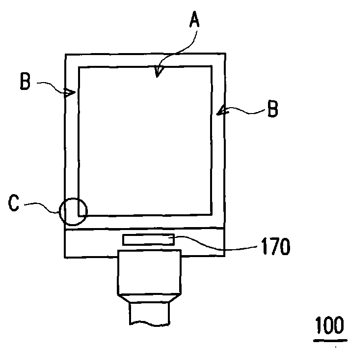
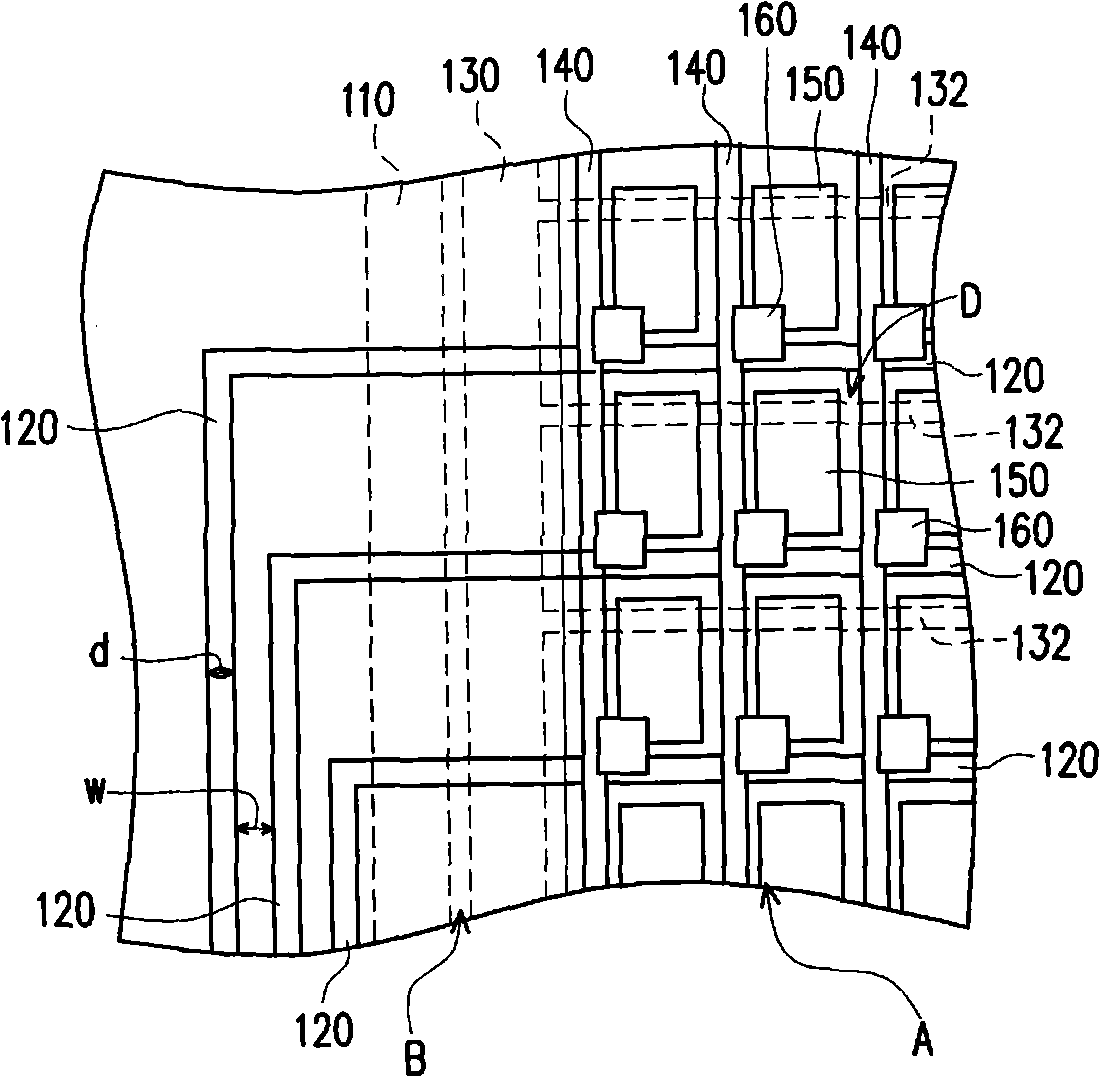
Active component array substrate and liquid crystal display panel technical field The invention belongs to the technical field of liquid crystal display, and in particular relates to an active component array substrate and a liquid crystal display panel. Background technique Today's display technology is quite developed, mostly benefiting from the progress of semiconductor technology and optoelectronic technology. As far as the display panel is concerned, the Liquid Crystal Display panel (LCD panel) is the most popular with the advantages of thinness, lightness, power saving, no radiation, full color, and portability. FIG. 1 is a schematic diagram of a known liquid crystal display panel. FIG. 2 is a partially enlarged view of the area C of the liquid crystal display panel of FIG. 1 , which shows the circuit of the active component array substrate of the liquid crystal display panel 100 . Please refer to FIG. 1 and FIG. 2 at the same time. The liquid crystal display pan...
Claims
Login to View More Application Information
Patent Timeline
 Patent Type & Authority Patents(China)
IPC IPC(8): H01L27/12H01L23/528G02F1/1362
Inventor 刘梦骐
Owner CPT TECH GRP
Features
- R&D
- Intellectual Property
- Life Sciences
- Materials
- Tech Scout
- Unparalleled Data Quality
- Higher Quality Content
- 60% Fewer Hallucinations
Learn More Browse by: Latest US Patents, China's latest patents, Technical Efficacy Thesaurus, Application Domain, Technology Topic, Popular Technical Reports.
© 2025 PatSnap. All rights reserved.Legal|Privacy policy|Modern Slavery Act Transparency Statement|Sitemap|About US| Contact US: help@patsnap.com