Light emitting diode (LED) encapsulation module

A technology of light-emitting diodes and molding, which is applied in the direction of electrical components, electric solid-state devices, circuits, etc., and can solve the problems of limited application level and large volume

Inactive Publication Date: 2009-09-16
林文达 +1
View PDF0 Cites 1 Cited by
  • Summary
  • Abstract
  • Description
  • Claims
  • Application Information

AI Technical Summary

Problems solved by technology

Because the traditional LED packaging module 100 has the above-mentioned substrate 110, the conventional LED packaging module 100 is often limited in its application level due to its large volume.

Method used


Image

  • Light emitting diode (LED) encapsulation module
  • Light emitting diode (LED) encapsulation module
  • Light emitting diode (LED) encapsulation module

Examples


Embodiment Construction

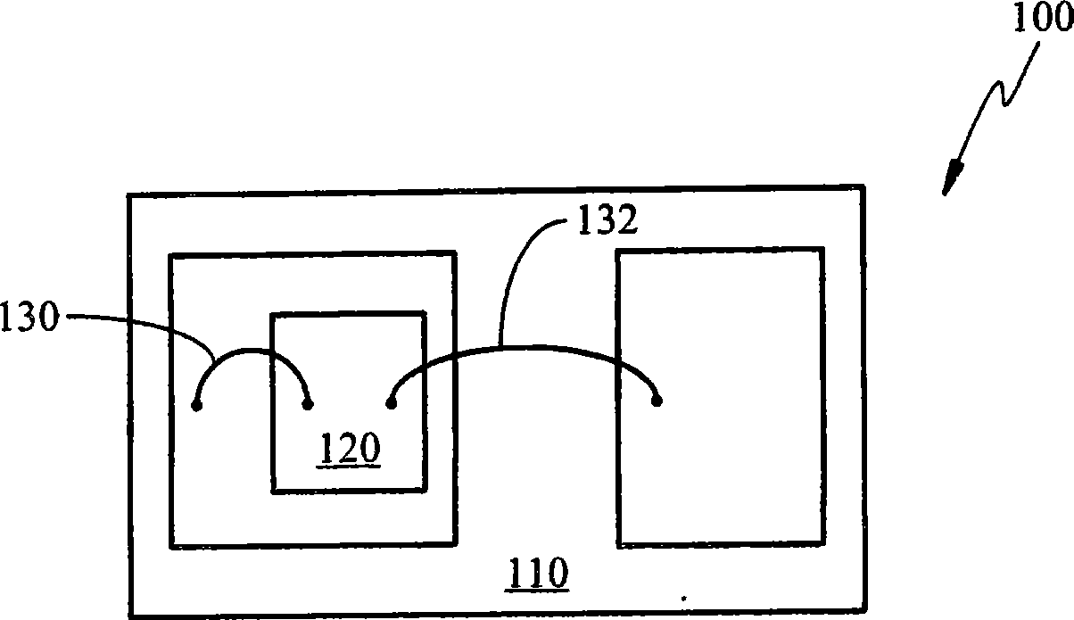
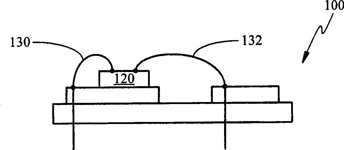
[0074] The direction of the present invention discussed here is a light emitting diode packaging module. In order to provide a thorough understanding of the present invention, detailed steps and components thereof will be set forth in the following description. Obviously, the implementation of the present invention is not limited to specific details familiar to those skilled in LED packaging modules. On the other hand, well-known components or steps have not been described in detail so as not to unnecessarily limit the invention. The preferred embodiments of the present invention will be described in detail as follows, but in addition to these detailed descriptions, the present invention can also be widely implemented in other embodiments, and the scope of the present invention is not limited, and it is subject to the scope of the following patents .

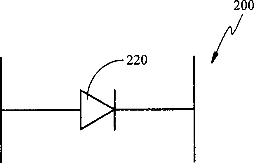
[0075] Because the light-emitting diode packaging module produced by the traditional COB packaging method must have a substr...


PUM


Abstract

The invention provides an LED encapsulation module comprising a first lead wire, a second lead wire and an LED crystal grain, wherein the LED crystal grain comprises a first electrode and a second electrode. The LED crystal grain is configured on the second lead wire, and the second electrode of the LED crystal grain is electrically coupled to the second lead wire, wherein the first electrode of the LED crystal grain is electrically coupled to the first lead wire by a first connecting wire.

Description

technical field [0001] The invention relates to a light emitting diode, in particular to a light emitting diode packaging module. Background technique [0002] In integrated circuit packaging technology, there is a direct chip packaging (Chip on Board, COB) technology, which is to directly stick the bare chip on the circuit board or substrate, and combine three basic processes: (1) chip adhesion (2 ) wire connection (3) application of sealing glue technology, effectively transfer the packaging and testing steps in the IC manufacturing process to the circuit board assembly stage. The COB (Chip on Board) packaging method is used in various modern electronic products, such as computers, mobile phones, clocks, toys, calculators and other daily necessities. [0003] refer to Figure 1A and Figure 1B As shown, it is a structural schematic diagram of a traditional light emitting diode packaging module 100 packaged by the above-mentioned COB technology. The above-mentioned conve...

Claims


Application Information

Patent Timeline
Patent Type & Authority Applications(China)
IPC IPC(8): H01L33/00H01L23/488H01L21/60H01L25/16
CPCH01L2224/49109H01L2224/48257H01L2224/48091H01L2224/73265
Inventor 林文达
Owner 林文达
Why Eureka
Try Eureka