Light emitting diode surface light source device

A technology of light-emitting diodes and surface light sources, applied in the directions of plane light sources, light sources, point light sources, etc.

Active Publication Date: 2009-09-30
BRIGHT LED ELECTRONICS CORP
View PDF0 Cites 9 Cited by
  • Summary
  • Abstract
  • Description
  • Claims
  • Application Information

AI Technical Summary

Problems solved by technology

[0005] The purpose of the present invention is to overcome the problems existing in the existing light-emitting diode surface light source device, and provide a light-emitting diode surface light source device with a small-sized wafer of a new structure. The technical problem to be sol...

Method used


Image

  • Light emitting diode surface light source device
  • Light emitting diode surface light source device
  • Light emitting diode surface light source device

Examples


Embodiment Construction

[0036] In order to further explain the technical means and effects of the present invention to achieve the intended purpose of the invention, the specific implementation, structure, features and Efficacy, as detailed below.

[0037] The foregoing and other technical contents, features and effects of the present invention will be clearly presented in the following detailed description of the preferred embodiment with reference to the drawings. Through the description of the specific embodiments, it is possible to gain a more in-depth and specific understanding of the technical means and effects adopted by the present invention to achieve the predetermined purpose. However, the accompanying drawings are only for reference and explanation purposes, and are not used for the present invention. Be restricted.

[0038] The following describes the present invention in detail with reference to the drawings and a specific embodiment:

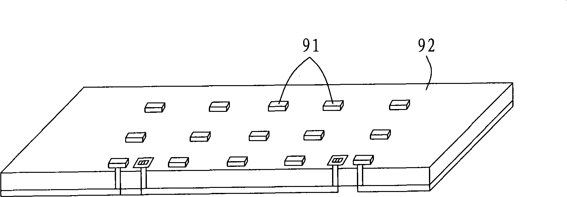
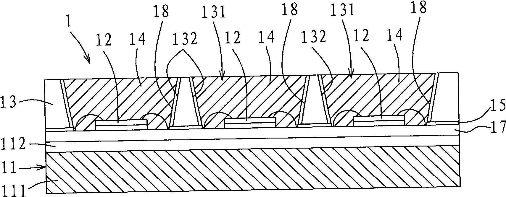
[0039] See figure 2 Shown is a cross-sectional view of...


PUM

PropertyMeasurementUnit
Thicknessaaaaaaaaaa

Abstract

The invention relates to a light emitting diode surface light source device, which comprises a substrate and a plurality of light emitting diode chips arranged on the substrate in array type arrangement. The thickness of the substrate is more than 1 mm. The area of the light emitting diode chip is between 0.08 and 0.25 mm <2>; and the distance between every two light emitting diode chips is more than twice of the dimension of the chip. The light emitting diode surface light source device uses the chip with small dimension and controls the distance between the chips and the thickness of the substrate, can achieve the promotion of luminous efficiency of the whole surface light source device through utilization of the chip with the small dimension, can maintain the temperature of the chip in a lower state, reduce the amplitude needed for radiation and is further favorable for the following radiation design of the whole light emitting diode surface light source device.

Description

Technical field [0001] The invention relates to a light-emitting diode device, in particular to a light-emitting diode surface light source device in which a plurality of light-emitting diodes are arranged as a surface light source. Background technique [0002] See figure 1 Shown is a three-dimensional schematic diagram of the prior art Taiwan bulletin number 289947. In the case of Taiwan Announcement No. 289947, what is disclosed is a technology in which a large number of light-emitting diode chips 91 (hereinafter referred to as chips) are arranged on a substrate 92 to form a surface light source, and the size of the chip 91 is less than 40 mils (especially in 8mil~14mil), thereby increasing the light extraction efficiency and improving the thermal conductivity. [0003] However, in fact, in addition to the size of the wafer 91, the distance between the wafers 91 and the thickness of the substrate 92 will also affect the heat dissipation of the entire surface light source, whi...

Claims


Application Information

Patent Timeline
IPC IPC(8): F21V21/00F21V29/00H01L23/373H01L33/00F21Y101/02F21V29/85F21Y105/12F21Y115/10
Inventor 张铭利陈炎成曾庆霖廖宗仁周政泰
Owner BRIGHT LED ELECTRONICS CORP
Why Eureka
Try Eureka