Process for Damascus
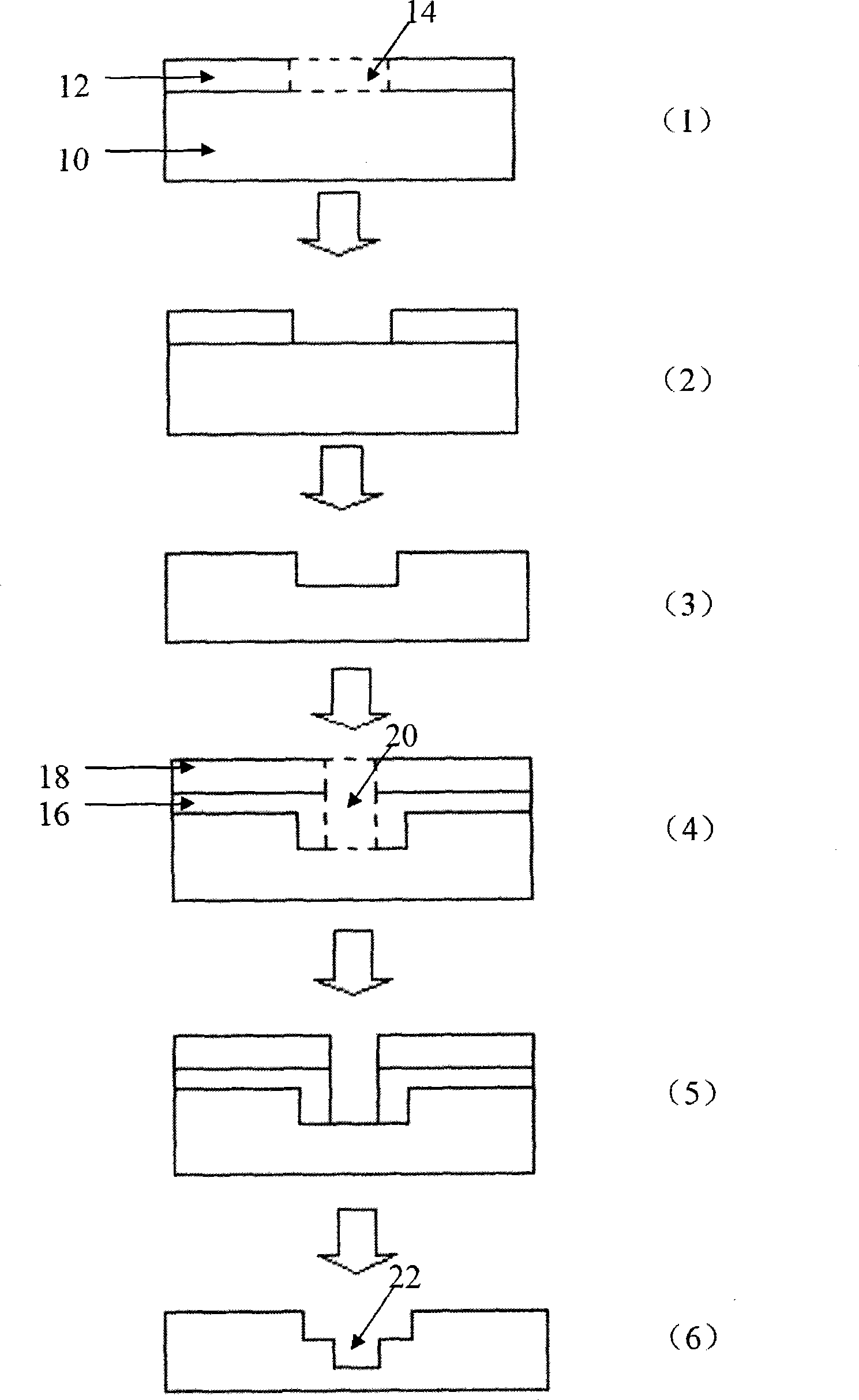
A process method and substrate technology, applied in the direction of electrical components, semiconductor/solid-state device manufacturing, circuits, etc., can solve problems such as low efficiency and complicated processing process, and achieve the effect of improving efficiency and reducing the number of times of development and etching
- Summary
- Abstract
- Description
- Claims
- Application Information
AI Technical Summary
Problems solved by technology
Method used
Image
Examples
Embodiment Construction
[0022] In order to make the purpose and features of the present invention more comprehensible, the specific implementation manners of the present invention will be further described below in conjunction with the accompanying drawings.
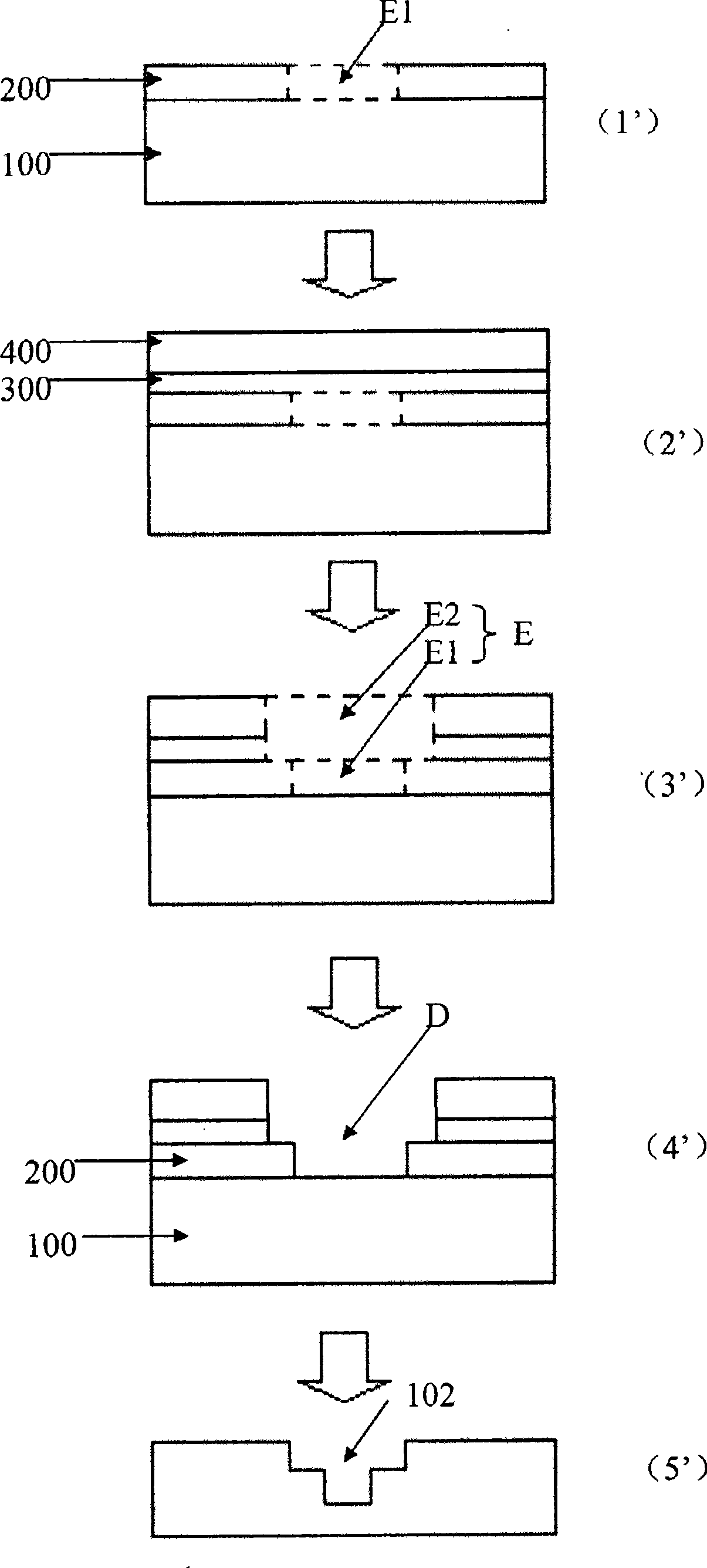
[0023] The damascene process method of the present invention can reduce the number of times of development and etching during the formation of the groove on the substrate (or the interlayer via hole on a dielectric layer), and it includes the following steps:
[0024] Continuously performing exposure treatment on a plurality of photoresist layers without developing treatment in between, thereby forming an exposure area;
[0025] performing a developing treatment on the exposed area to obtain a developed area corresponding to the exposed area;
[0026] The base or a dielectric layer is etched through the above-mentioned developing area to form the desired groove or through hole.
[0027] In order to better understand the present invention, the ...
PUM
 Abstract
Description
Claims
Application Information
 - R&D
- Intellectual Property
- Life Sciences
- Materials
- Tech Scout
- Unparalleled Data Quality
- Higher Quality Content
- 60% Fewer Hallucinations
Browse by: Latest US Patents, China's latest patents, Technical Efficacy Thesaurus, Application Domain, Technology Topic, Popular Technical Reports.
© 2025 PatSnap. All rights reserved.Legal|Privacy policy|Modern Slavery Act Transparency Statement|Sitemap|About US| Contact US: help@patsnap.com


