Semiconductor device

a technology of semiconductor integrated circuits and capacitors, applied in the direction of power consumption reduction, pulse techniques, instruments, etc., can solve the problems of power consumption, unnecessary power consumption in basic blocks, and power consumption is expected to increase, so as to suppress the degradation of gate insulating films, suppress the number of times of rewriting data, and reduce the effect of power consumption

Active Publication Date: 2013-10-01
SEMICON ENERGY LAB CO LTD
View PDF149 Cites 96 Cited by
  • Summary
  • Abstract
  • Description
  • Claims
  • Application Information

AI Technical Summary

Benefits of technology

[0005]Conventionally, in semiconductor integrated circuits such as a normal central processing unit (CPU), the circuits are designed in advance and cannot be changed after manufacturing. In contrast, in a semiconductor integrated circuit called a programmable logic device (PLD), a logic circuit is formed using basic block units having an adequate structure and interconnections between the basic block units can be changed after manufacturing. Therefore, the PLD has high versatility because a circuit configuration can be changed by a user, and the time and cost spent on design and development of a circuit can be greatly reduced.

Problems solved by technology

However, power supply voltage is supplied also to the basic blocks which do not contribute to the circuit configuration in the PLD.
Therefore, in the basic blocks, various capacitance including parasitic capacitance are charged and discharged wastefully, so that power is consumed.
When the power supply voltage is supplied, unnecessary power consumption occurs in the basic blocks due to leakage current or off-state current.
In the case where a CMOS inverter is formed using bulk silicon, an off-state current of approximately 1 pA is generated at a room temperature with a power supply voltage of approximately 3 V. When high integration of the PLD is achieved, power consumption is expected to be increased due to miniaturization of a semiconductor element or an increase in the number of elements.
However, since the EEPROM writes and erases data utilizing the principle of tunneling current, deterioration of an insulating film easily occurs.
Accordingly, in practice, the number of times of rewriting data is not infinite, and the upper limit of the number of rewritings is approximately tens of thousands of times to hundreds of thousands of times. In addition, an absolute value of the voltage applied to the EEPROM when data is written and when data is erased is as high as around 20 V. Therefore, power consumption easily increases when data is written and when data is erased.
In addition, a redundant circuit design for covering the size of the above operating voltage is necessary.

Method used


Image

  • Semiconductor device
  • Semiconductor device
  • Semiconductor device

Examples


embodiment 1

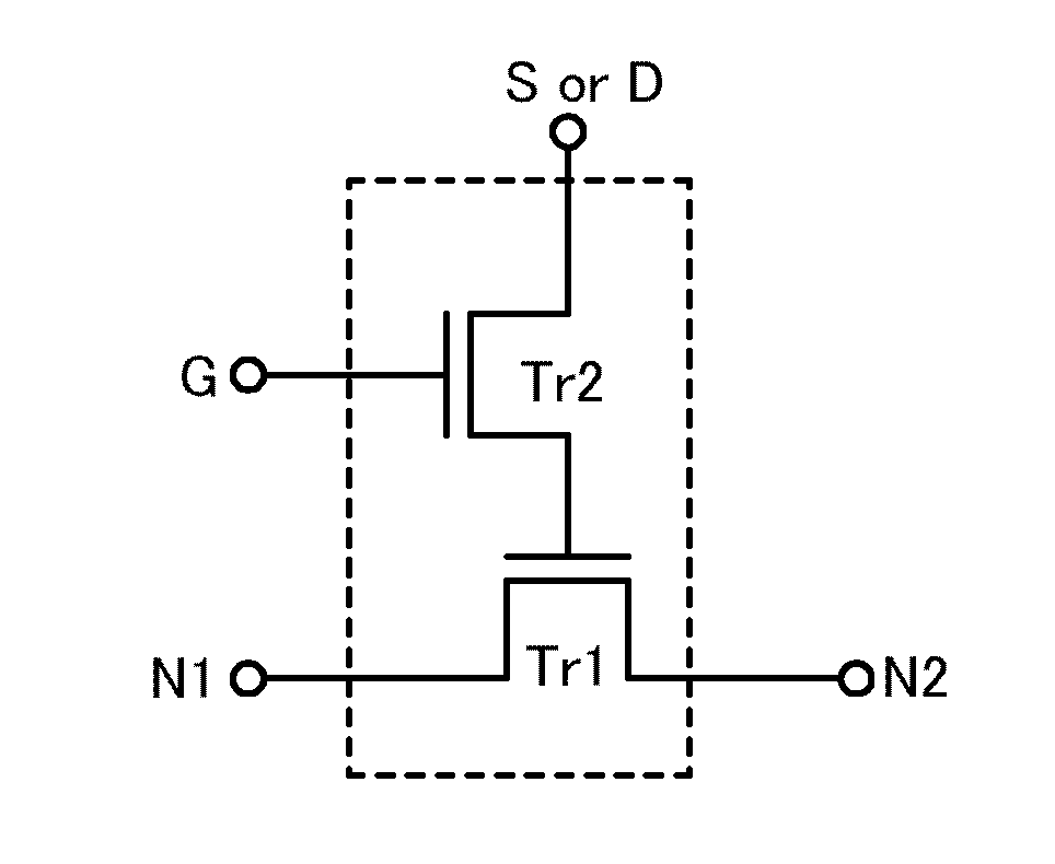
[0045]In this embodiment, a structure and operation of a semiconductor device according to one embodiment of the present invention will be described.

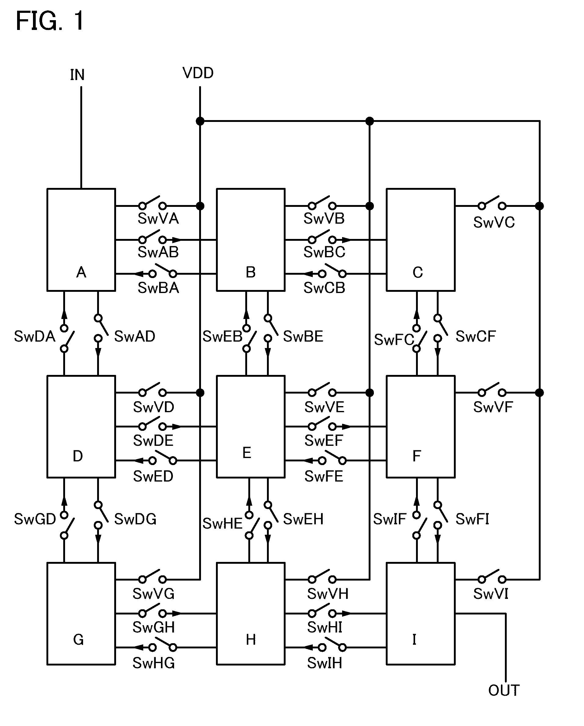
[0046]A structure of a semiconductor device according to one embodiment of the present invention is illustrated in FIG. 1, as an example. The semiconductor device illustrated in FIG. 1 is provided with nine basic blocks A to I, programming cells SwAB to SwIH configured to control connections between the basic blocks A to I, and programming cells SwVA to SwVI configured to control the supply of a power supply potential VDD to the basic blocks A to I.

[0047]Note that in FIG. 1, a programming cell configured to control a connection between an output terminal of the basic block A and an input terminal of the basic block B is denoted as SwAB, for example. On the other hand, a programming cell configured to control a connection between an output terminal of the basic block B and an input terminal of the basic block A is denoted as SwBA.

[0048]I...

embodiment 2

[0093]In Embodiment 1, the example in which a given basic block can be connected to up to four adjacent basic blocks is described; however, in this embodiment, an example in which a given basic block is connected to eight adjacent basic blocks will be described.

[0094]In a manner similar to that of FIG. 1, a semiconductor device illustrated in FIG. 6 is provided with nine basic blocks A to I, programming cells which control connections between the basic blocks A to I, and programming cells which control the supply of the power supply potential VDD to each of the basic blocks A to I.

[0095]Unlike FIG. 1, in the semiconductor device illustrated in FIG. 6, the central basic block E can be connected to all the basic blocks except the basic block E, via programming cells SwAE to SwIE and programming cells SwEA to SwEI.

[0096]Note that in FIG. 6, only the programming cells SwAE to SwIE which control connections between the central basic block E and the other basic blocks, the programming cel...

embodiment 3

[0100]A semiconductor device in which a large matrix is formed using basic blocks will be described using an example which is more generalized.

[0101]In this embodiment, attention is paid on a basic block U(n, m) of the n-th row and the m-th column included in the semiconductor device. As illustrated in FIG. 7, around the basic block U(n, m), there are eight basic blocks: U(n−1, m−1); U(n, m−1); U(n+1, m−1); U(n−1, m); U(n+1, m); U(n−1, m+1); U(n, m+1); and U(n+1, m+1). The basic block U(n, m) is connected to these eight basic blocks via programming cells in order to transmit and receive signals.

[0102]In FIG. 8, an example of a specific structure of a programming cell for controlling connections between the basic blocks illustrated in FIG. 7 and a programming cell for controlling the supply of the power supply potential VDD to each basic block is illustrated.

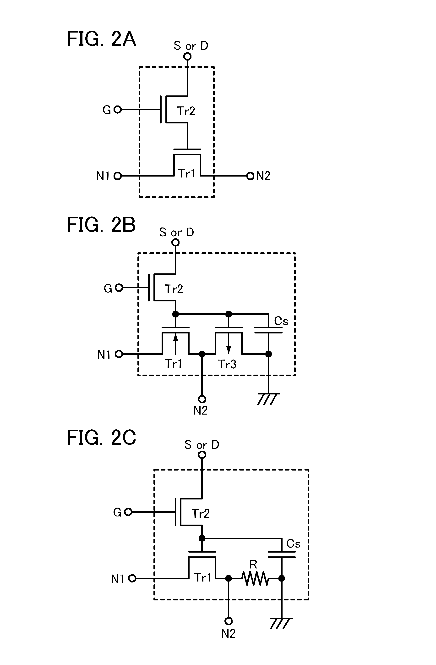
[0103]Note that an example in which the programming cell illustrated in FIG. 2A is used is described in FIG. 8; however, any of...


PUM


Abstract

It is an object to provide a semiconductor device in which power consumption can be reduced. It is another object to provide a highly reliable semiconductor device using a programming cell, such as a programmable logic device (PLD). In accordance with a change in a configuration of connections between basic blocks, power supply voltage furnishing to the basic blocks is changed. That is, when the structure of connections between the basic blocks is such that a basic block does not contribute to a circuit, the supply of the power supply voltage to this basic block is stopped. Further, the supply of the power supply voltage to the basic blocks is controlled using a programming cell formed using a field effect transistor whose channel formation region is formed using an oxide semiconductor, the field effect transistor having extremely low off-state current or extremely low leakage current.

Description

TECHNICAL FIELD[0001]The present invention relates to a semiconductor device including a semiconductor element using an oxide semiconductor.BACKGROUND ART[0002]In recent years, a metal oxide exhibiting semiconductor characteristics and called oxide semiconductor has attracted attention as a novel semiconductor material having higher mobility and higher reliability than amorphous silicon, and having uniform element characteristics. Metal oxides are used for various applications. For example, indium oxide is a well-known metal oxide and used as a material of a transparent electrode included in a liquid crystal display device or the like. Examples of such metal oxides having semiconductor characteristics include tungsten oxide, tin oxide, indium oxide, and zinc oxide. Thin film transistors whose channel formation region is formed using such a metal oxide having semiconductor characteristics are known (Patent Documents 1 and 2).REFERENCE[0003][Patent Document 1] Japanese Published Paten...

Claims


Application Information

Patent Timeline
Patent Type & Authority Patents(United States)
IPC IPC(8): G11C11/34G11C16/06
CPCH03K19/17784H03K19/17736H03K19/17772H03K19/173H01L29/7869H01L2924/0002H01L2924/00H03K19/0013H03K19/17724H03K19/1776H01L27/1225H01L27/0629H03K17/161
Inventor TAKEMURA, YASUHIKOYAMAZAKI, SHUNPEI
Owner SEMICON ENERGY LAB CO LTD
Why Eureka
Try Eureka