Switch panel and liquid crystal display system for three-dimensional display device

A switch panel, three-dimensional display technology, applied in static indicators, instruments, optics, etc., can solve the problems of complex technology, complex control technology, difficult to achieve, etc., to achieve the effect of simple driving method, overcoming complex structure, and simple structure

Active Publication Date: 2009-10-14
K TRONICS (SUZHOU) TECH CO LTD +1
View PDF5 Cites 25 Cited by
  • Summary
  • Abstract
  • Description
  • Claims
  • Application Information

AI Technical Summary

Problems solved by technology

However, this method also has certain defects. It is necessary to use a modulated polarizer as the switch panel, so the manufacture of the polarizer is difficult and costly, and the control technology is complicated, so it is difficult to realize
[0006] Through the analysis of the existing technology, it can be seen that most of the existing display devices with three-dimensional imaging function have the problems of complicated technology, high cost, inconvenient production and use, and there is also the problem that binocular images cannot be strictly distinguished, resulting in three-dimensional imaging effects. bad

Method used


Image

  • Switch panel and liquid crystal display system for three-dimensional display device
  • Switch panel and liquid crystal display system for three-dimensional display device
  • Switch panel and liquid crystal display system for three-dimensional display device

Examples


Embodiment 2

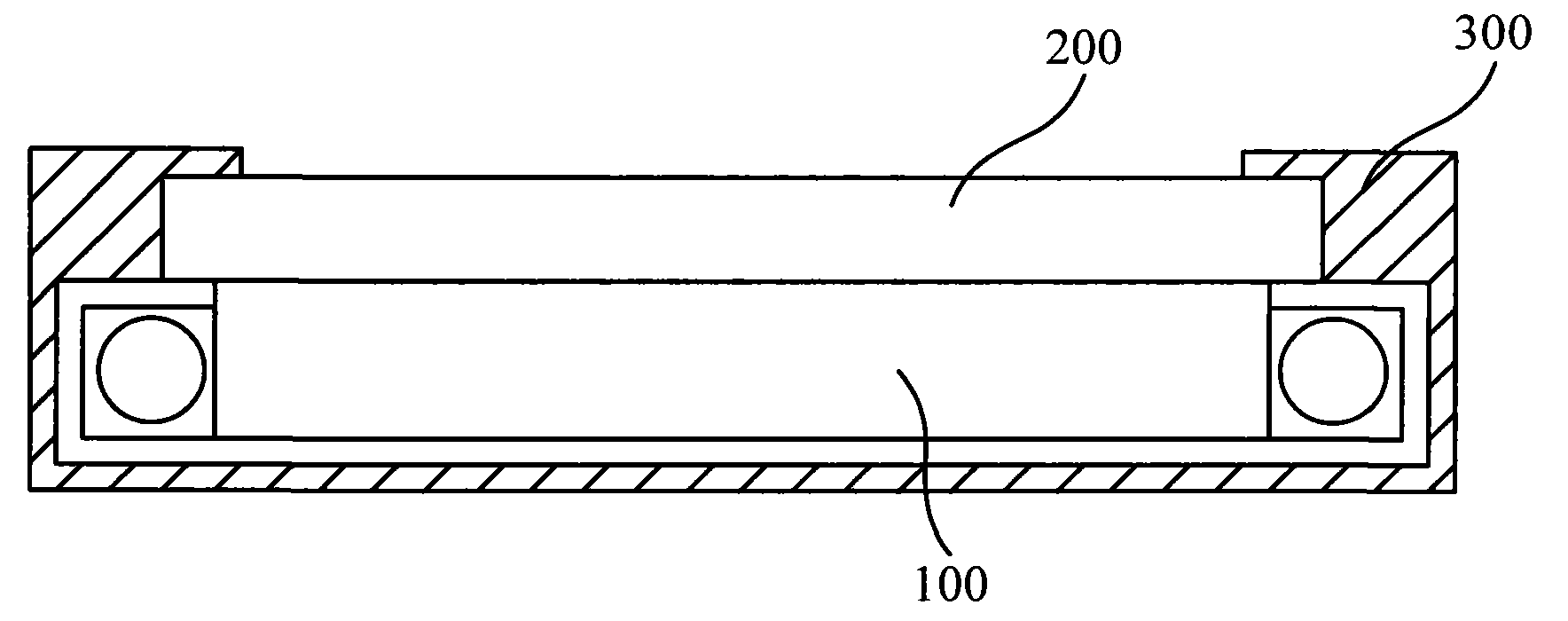
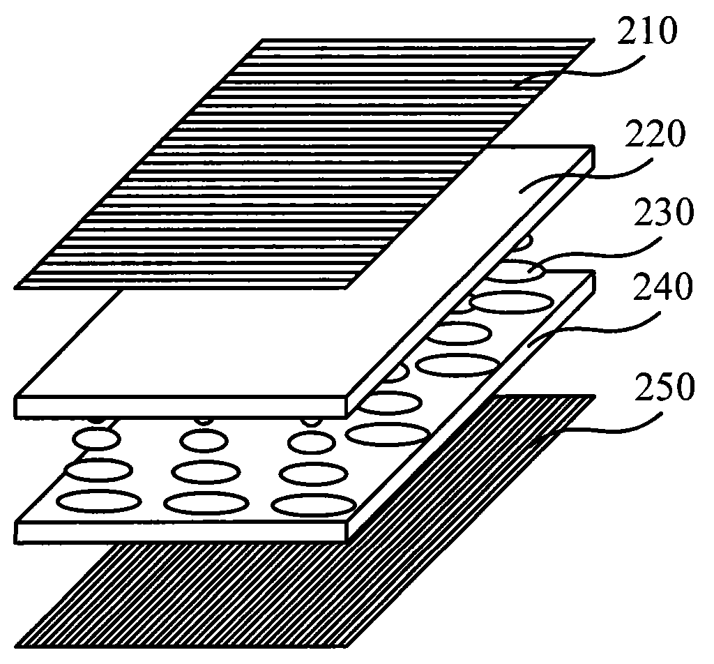
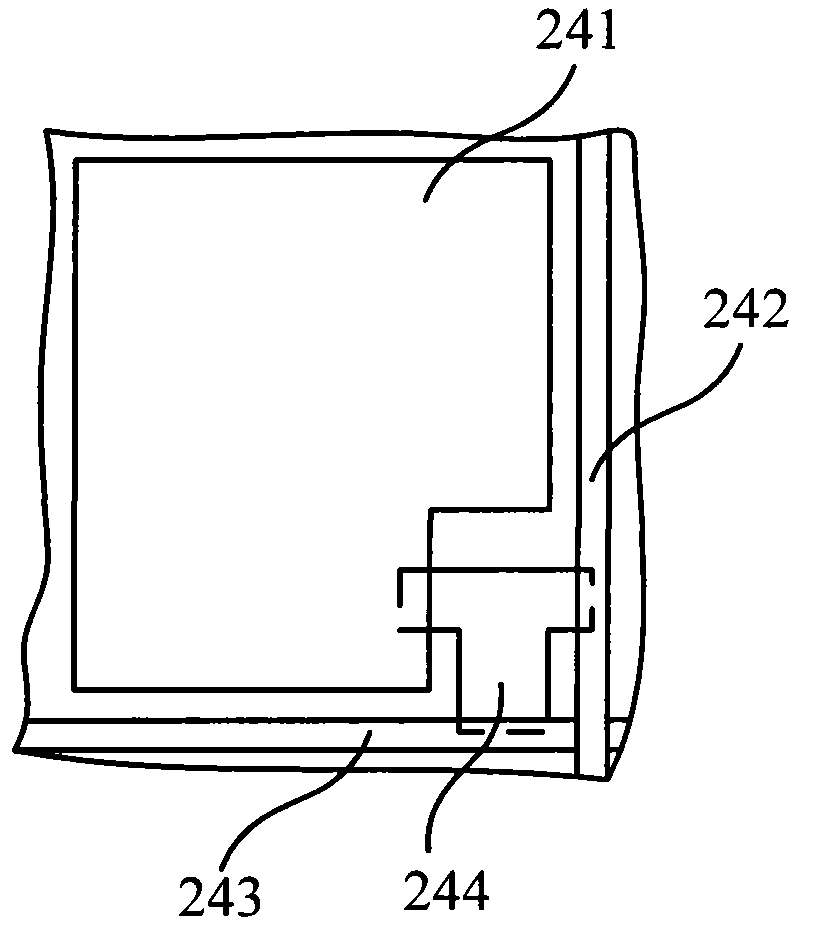
[0043] The difference between the technical solution of the second embodiment of the switch panel for a three-dimensional display device of the present invention and the first embodiment is that the transparent conductive film may not be a uniformly laid film, but may be composed of conductive regions arranged in a matrix. The conductive regions Corresponding to the pixel units on the array substrate. Further, the structure of the first transparent substrate and the transparent conductive film and the first alignment film on it may be the same as that of the array substrate, that is, the glass substrate of the array substrate is used as the first transparent substrate, and the pixel electrodes on the array substrate are used as the transparent conductive film. The alignment film attached on the array substrate serves as the first alignment film.

[0044] Compared with the first embodiment, the technical solution of this embodiment has the advantage that the existing prepared a...


PUM


Abstract

The invention relates to a switch panel and a liquid crystal display system for a three-dimensional display device. The switch panel and a light emergent side of a polaroid portrait of the liquid crystal device are arranged in an attaching way; the switch panel comprises two transparent substrates; transparent conductive films are respectively coated on two opposite surfaces of the two transparent substrates; a liquid crystal layer is filled between the two transparent substrates; and oriented films mutually vertical to oriented grooves are respectively arranged on two sides of the two transparent substrate. The other switch panel and the light emergent side of a polaroid portrait of the liquid crystal device are arranged in an attaching way; the switch panel comprises at least one transparent substrate, liquid crystal layers filled between the transparent substrate and the liquid crystal display device, and two transparent electrodes on which driving signals are applied; the oriented films are arrayed along a first mode; and the liquid crystal layers are arrayed along a second mode. The liquid crystal display system comprises the switch panel and polarization analyzing glass which corresponds to the switch panel. The invention adopts a liquid crystal secondary optical rotation technology to achieve three-dimensional image and has simple structure, low cost and favorable imaging effect.

Description

technical field [0001] The invention relates to a switch panel and a liquid crystal display system for a three-dimensional display device, in particular to a switch panel capable of enabling the display device to display a three-dimensional image, and a liquid crystal display system including the switch panel. Background technique [0002] Liquid crystal display is the mainstream product in current flat panel display devices. The general structure of liquid crystal display, especially Thin Film Transistor-Liquid Crystal Display (hereinafter referred to as TFT-LCD) is as follows: figure 1 As shown, it consists of four parts: a backlight module 100, a liquid crystal panel, an outer frame 300 and an image signal driving device (not shown in the figure). Because the existing liquid crystal panel mainly plays a display role, it can also be called a liquid crystal display panel, that is, a liquid crystal display device 200 that emits polarized images. Wherein, the backlight modul...

Claims


Application Information

Patent Timeline
Patent Type & Authority Applications(China)
IPC IPC(8): G02F1/133G02B27/26G02B30/25
Inventor 刘海军金哲润尹大根宋冠男
Owner K TRONICS (SUZHOU) TECH CO LTD
Why Eureka
Try Eureka