Array substrate of capacitance type liquid crystal display device on grid line
A liquid crystal display device, array substrate technology, applied in the direction of circuits, electrical components, static indicators, etc., can solve problems such as defects, achieve high picture quality, overcome defects, and improve quality
- Summary
- Abstract
- Description
- Claims
- Application Information
AI Technical Summary
Problems solved by technology
Method used
Image


Examples
no. 1 example
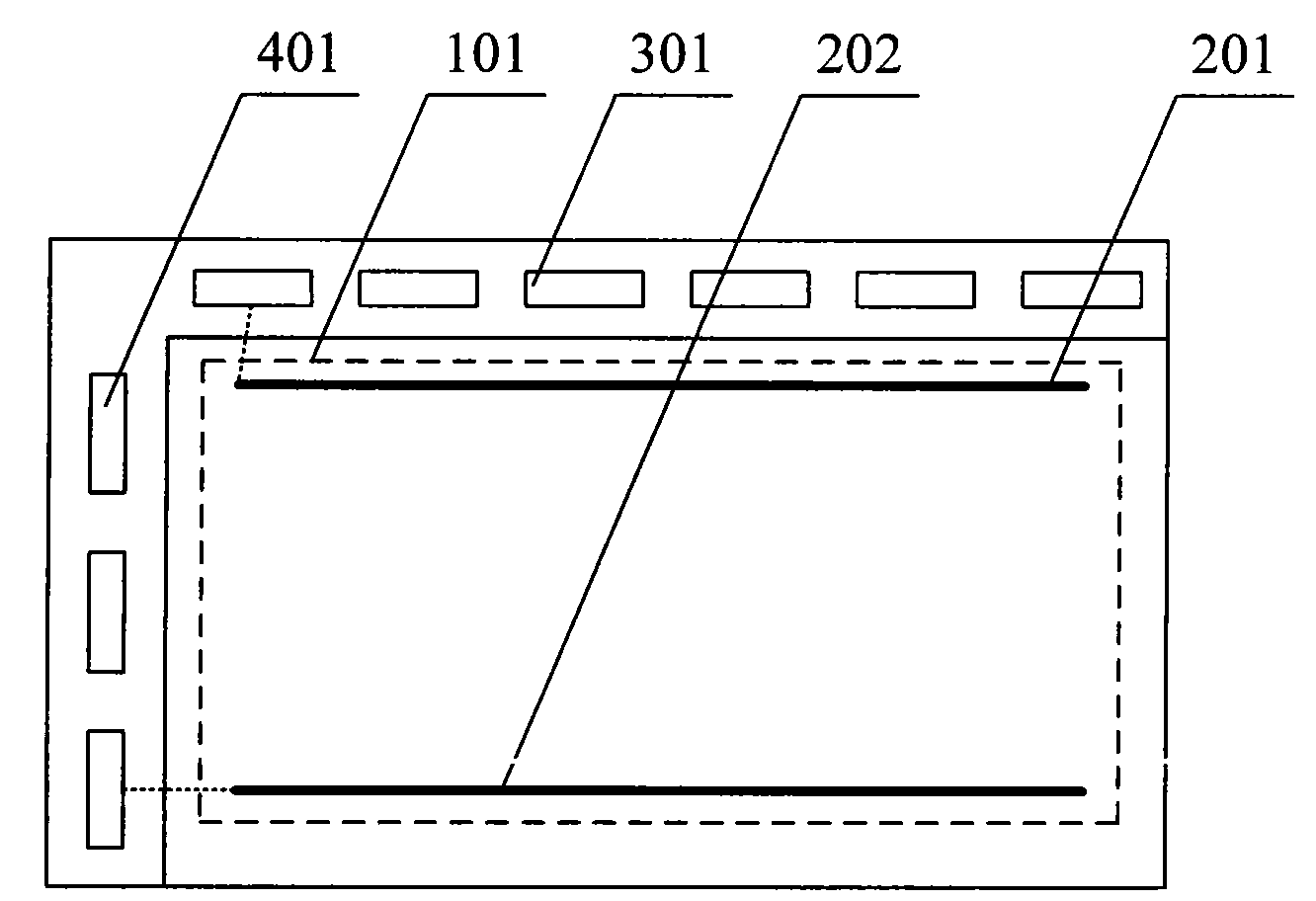
[0024] figure 2 It is a structural schematic diagram of the first embodiment of the present invention, such as figure 2 As shown, the liquid crystal display device mainly includes a panel composed of a relatively large array substrate and a relatively small color filter substrate. The array substrate forms a storage capacitor by means of capacitance on the gate line, and the panel is provided with a display area And the non-display area 101, M*N pixels (M and N are both integers) are arranged on the display area 101, the non-display area is located around the display area 101, and is divided into: the first one located on the left side of the display area 101 a side non-display area, a second side non-display area located below the display area 101 , a third side non-display area located to the right of the display area 101 , and a fourth side non-display area located above the display area 101 . No. 0 to No. N gate lines are provided in the display area 101 , and gate inpu...
no. 2 example
[0030] image 3 It is a structural schematic diagram of the second embodiment of the present invention, such as image 3 As shown, the liquid crystal display device mainly includes a panel composed of a relatively large array substrate and a relatively small color filter substrate. The array substrate forms a storage capacitor by means of front-end gate lines, wherein the gate of the gate line driver 401 The total number of input terminals (at least N+1) is greater than or equal to the total number of gate lines of the array substrate, wherein the panel is provided with a display area and a non-display area 101, and M*N pixels are provided on the display area 101 (M and N are both Integer), the non-display area is located around the display area 101, and is divided into: a first-side non-display area located on the left side of the display area 101, a second-side non-display area located on the lower side of the display area 101, and a second-side non-display area located on t...
PUM
 Abstract
Description
Claims
Application Information