Circuit board and manufacture method thereof

A manufacturing method and circuit board technology, applied in the direction of multilayer circuit manufacturing, printed circuit components, electrical components, etc., can solve problems such as electromagnetic interference and serious noise

Active Publication Date: 2009-10-21
UNIMICRON TECH CORP
View PDF0 Cites 1 Cited by
  • Summary
  • Abstract
  • Description
  • Claims
  • Application Information

AI Technical Summary

Problems solved by technology

However, as the frequency of electrical signals transmitted by the line layer becomes higher and higher, the electromagnetic interference and noise between any two line layers will become more and more serious

Method used


Image

  • Circuit board and manufacture method thereof
  • Circuit board and manufacture method thereof
  • Circuit board and manufacture method thereof

Examples


Embodiment Construction

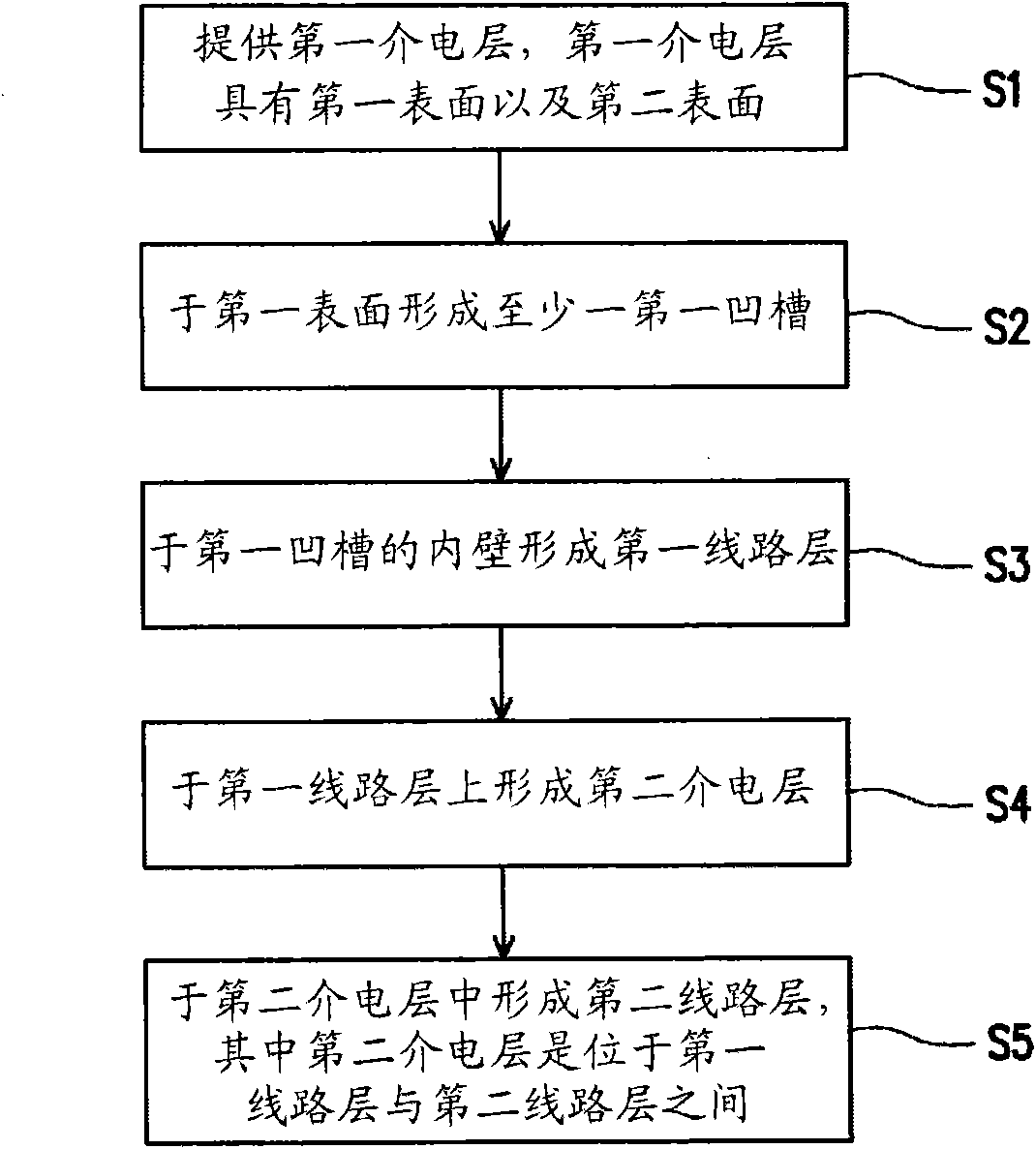
[0025] figure 1 A flow chart of manufacturing a circuit board according to an embodiment of the present invention is shown. Please refer to figure 1 , in this embodiment, the manufacturing method of the circuit board includes the following steps: First, as shown in step S1, a first dielectric layer is provided, and the first dielectric layer has a first surface and a second surface. Then, as shown in step S2, at least one first groove is formed on the first surface. Next, as shown in step S3, a first circuit layer is formed on the inner wall of the first groove. Next, as shown in step S4, a second dielectric layer is formed on the first circuit layer. After that, as shown in step S5 , a second circuit layer is formed in the second dielectric layer, wherein the second dielectric layer is located between the first circuit layer and the second circuit layer.

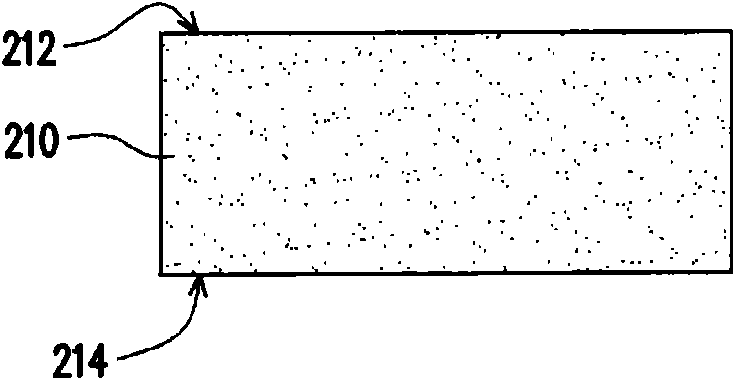
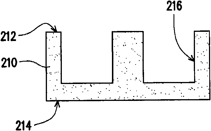
[0026] In order to understand the manufacturing method of the circuit board of this embodiment in more detail, this e...


PUM


Abstract

The invention discloses a circuit board which comprises a first dielectric layer, a first circuit layer, a second dielectric layer and a second circuit layer. The first dielectric layer is provided with a first surface and a second surface, wherein the first surface is provided with at least one groove. The first circuit layer is arranged on the inner wall of the groove. Furthermore, the second dielectric layer is arranged in the groove and covers the first circuit layer; the second circuit layer is arranged in the groove; and the second dielectric layer is positioned between the first circuit layer and the second circuit layer. The invention also discloses a manufacture method of the circuit board.

Description

technical field [0001] The invention relates to a circuit board and a manufacturing method thereof, in particular to a circuit board with electromagnetic shielding effect and a manufacturing method thereof. Background technique [0002] Generally speaking, a circuit board for carrying or electrically connecting multiple electronic components is composed of a plurality of patterned conductive layers and a plurality of dielectric layers stacked alternately. Wherein, these patterned circuit layers are formed by defining and etching copper foil layers through photolithography. The dielectric layers are respectively disposed between two adjacent patterned circuit layers to isolate the patterned circuit layers. In addition, various electronic components (such as active components or passive components) can also be arranged on the surface of the circuit board, and the purpose of electrical signal propagation can be achieved through other lines inside the circuit board. However, a...

Claims


Application Information

Patent Timeline
Patent Type & Authority Applications(China)
IPC IPC(8): H05K3/46H05K1/02H05K9/00
Inventor 余丞博余丞宏
Owner UNIMICRON TECH CORP
Why Eureka
Try Eureka