Substrate of circuit board and manufacturing method thereof

A board substrate, circuit board technology, applied in the direction of circuit substrate materials, printed circuit manufacturing, printed circuit, etc., can solve the problems of increasing the production cost of circuit boards, poor flexibility of stainless steel sheets, high price of stainless steel sheets, etc., to prevent ion migration , reduce production cost, increase the effect of flexural performance

Inactive Publication Date: 2012-03-14
AVARY HLDG (SHENZHEN) CO LTD +1
View PDF4 Cites 1 Cited by
  • Summary
  • Abstract
  • Description
  • Claims
  • Application Information

AI Technical Summary

Problems solved by technology

However, the weight of the stainless steel sheet is relatively large, thereby increasing the weight of the circuit board product
And the flexibility of the stainless steel sheet is poor, and the electromagnetic shielding layer made of stainless steel sheet affects the flexural performance of the flexible circuit board
Due to the high price of stainless steel sheets, the production cost of the circuit board is increased

Method used


Image

  • Substrate of circuit board and manufacturing method thereof
  • Substrate of circuit board and manufacturing method thereof
  • Substrate of circuit board and manufacturing method thereof

Examples


Embodiment Construction

[0023] The circuit board substrate provided by the technical solution and the manufacturing method thereof will be further described in detail below in conjunction with the embodiments.

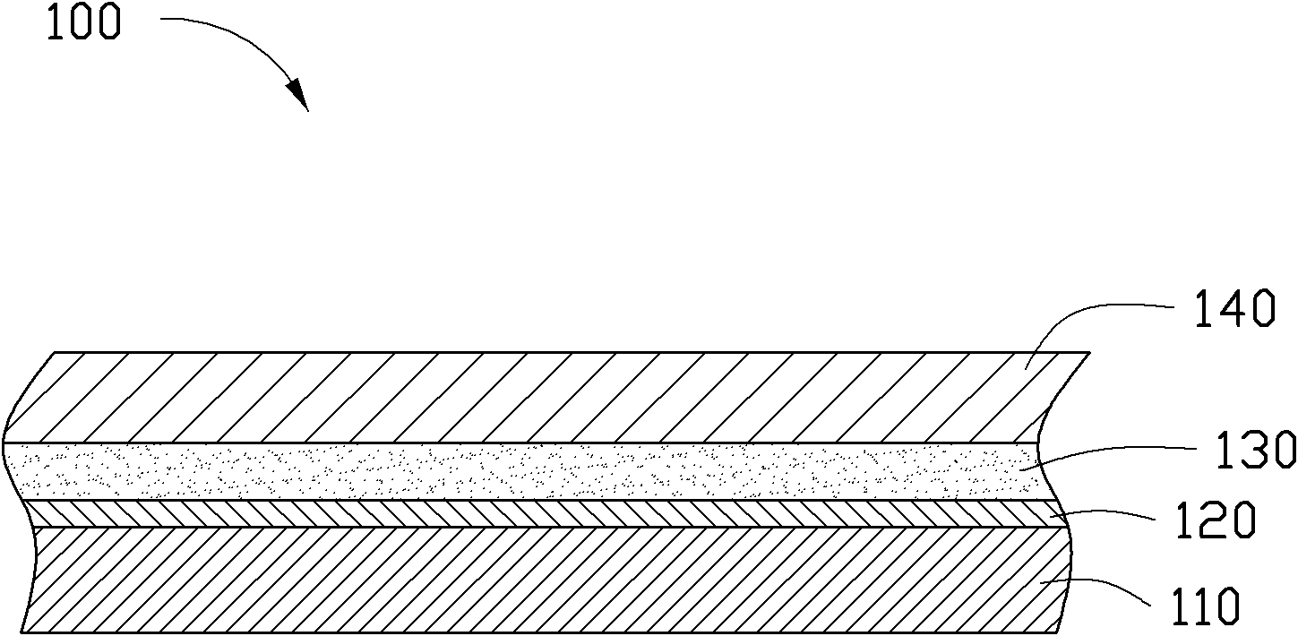
[0024] see figure 1 , The technical solution provides a circuit board substrate 100, which includes an insulating base material layer 110, an epoxy resin composite material layer 120, an adhesive layer 130, and a metal layer 140 stacked in sequence.

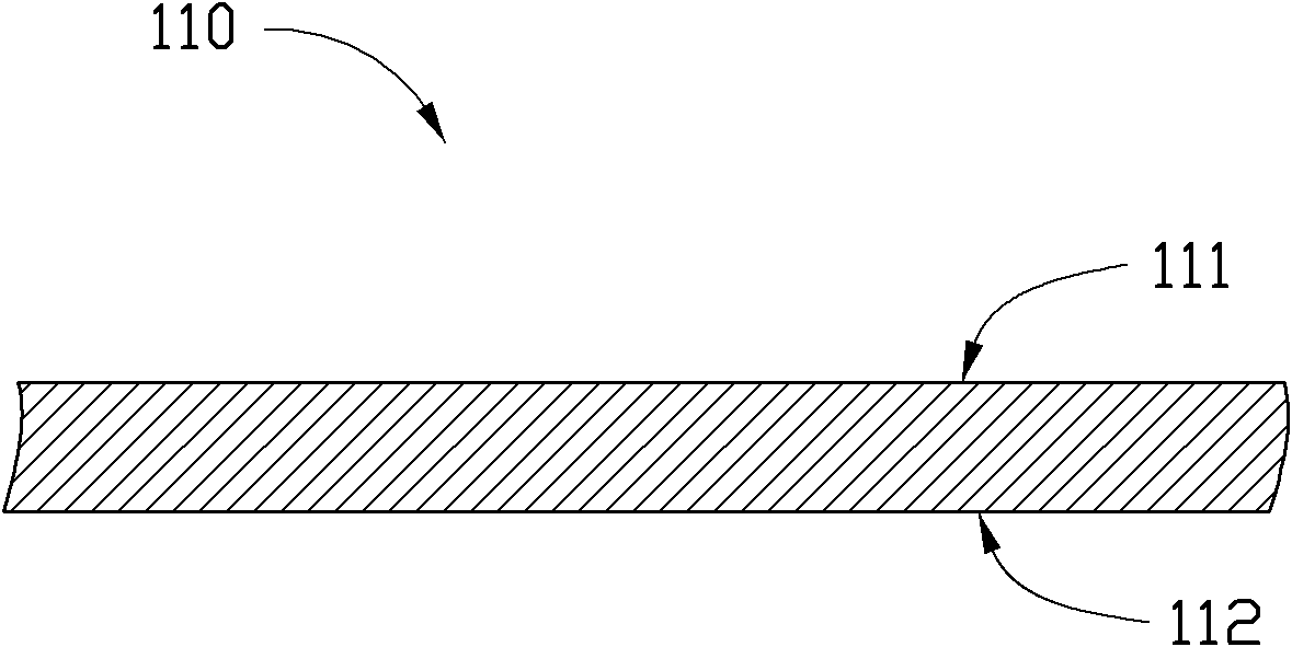
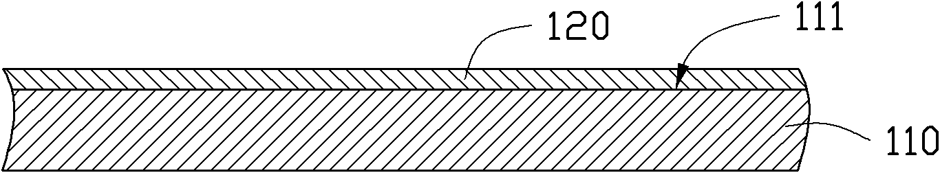
[0025] The insulating substrate layer 110 is used to carry the epoxy resin composite material layer 120 and play a role of electrical insulation. In this embodiment, the insulating base layer 110 is made of polyimide. The thickness of the insulating substrate layer 110 can be set according to actual needs, and its thickness can be 10 microns to 50 microns, preferably 25 microns.

[0026] The adhesive layer 130 is used to bond the epoxy resin composite material layer 120 and the metal layer 140 , and to electrically insulate the epoxy resin com...


PUM

PropertyMeasurementUnit
thicknessaaaaaaaaaa
thicknessaaaaaaaaaa
thicknessaaaaaaaaaa

Abstract

The invention relates to a substrate of a circuit board. The structure comprises an insulating base material layer, an epoxy resin composite material layer, an adhesive layer and a metal layer, which are sequentially stacked. The epoxy resin composite material layer is made of epoxy resin composite material. The epoxy resin composite material comprises epoxy resin modified by a carboxyl-terminated polymer, carbon nanotubes and inorganic dispersion material, wherein the carbon nanotubes account for 4.6% by weight to 16% by weight of the epoxy resin composite material. The invention further provides a manufacturing method of the substrate of the circuit board.

Description

technical field [0001] The invention relates to the technical field of circuit boards, in particular to a circuit board substrate applied to the production of circuit boards and having an electromagnetic shielding effect and a manufacturing method thereof. Background technique [0002] With the advancement of science and technology, printed circuit boards have been widely used in the electronic field. For the application of the circuit board, please refer to the literature Takahashi, A.Ooki, N.Nagai, A.Akahoshi, H.Mukoh, A.Wajima, M.Res.Lab, High density multilayer printed circuit board for HITAC M-880, IEEE Trans. on Components, Packaging, and Manufacturing Technology, 1992, 15(4): 418-425. [0003] As the number of layers of circuit board products increases, electromagnetic interference often occurs when the circuit board products are actually working, which affects the signal transmission of the circuit board. In this way, an electromagnetic shielding layer needs to be ...

Claims


Application Information

Patent Timeline
Patent Type & Authority Applications(China)
IPC IPC(8): H05K1/03H05K3/00H05K9/00B32B15/092B32B27/08B32B27/18B32B27/34C08L63/02C08K3/34C08K7/00C08K3/04
Inventor 何明展
Owner AVARY HLDG (SHENZHEN) CO LTD
Why Eureka
Try Eureka