Conductive substrate of large-area dye-sensitized solar cell and solar cell thereof
A technology of solar cells and dye sensitization, applied in the field of dye-sensitized solar cells, can solve the problems of increased electron loss, long electron transmission distance, etc.
- Summary
- Abstract
- Description
- Claims
- Application Information
AI Technical Summary
Problems solved by technology
Method used
Image
Examples
Embodiment Construction
[0017] In order to describe the technical content, structural features, achieved goals and effects of the present invention in detail, the following will be described in detail in conjunction with examples and diagrams.
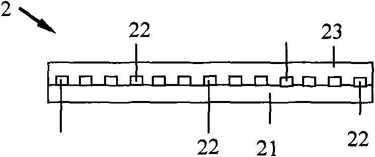
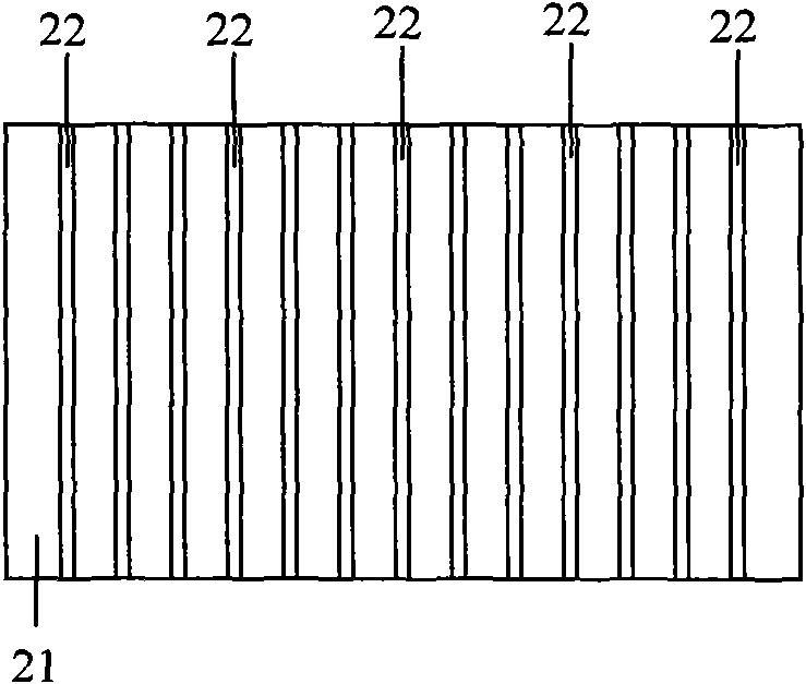
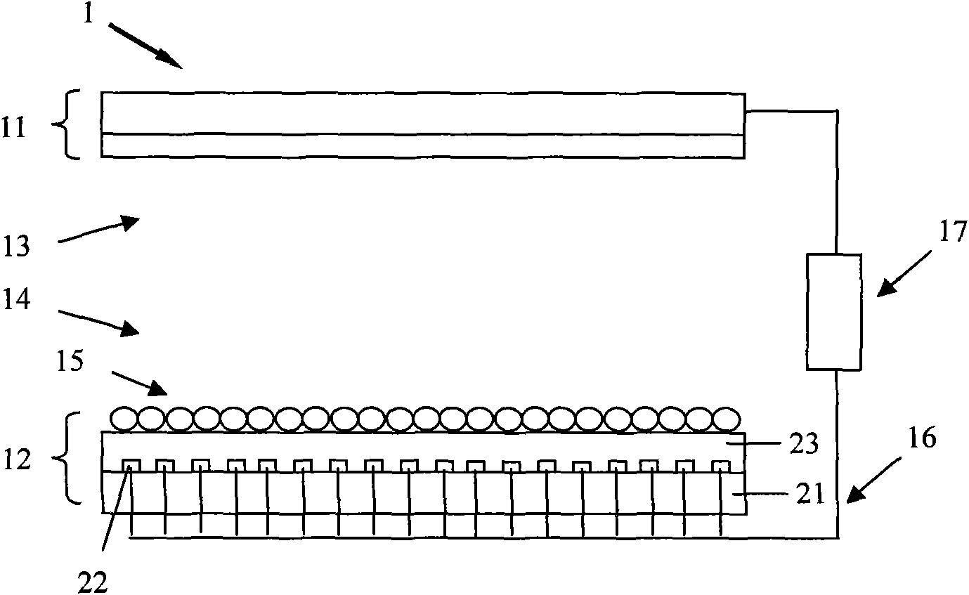
[0018] Please refer to FIG. 1( a ) and FIG. 1( b ). FIG. 1( a ) and FIG. 1( b ) show the conductive substrate 2 of the large-area dye-sensitized solar cell 1 . The conductive base 2 includes a transparent substrate 21 , a gate electrode 22 adjacent to the transparent substrate 21 and spaced apart on the transparent substrate 21 , and a conductive layer 23 coated on the transparent substrate 21 and covering the gate electrode 22 . The transparent substrate 21 is a transparent glass substrate or a transparent polymer substrate, including, but not limited to, an FTO glass substrate and an ITO / PET glass substrate. The gate electrode 22 is a conductive metal electrode. The width of the gate electrode 22 is 2-100 microns, preferably 20 microns. The distance betwe...
PUM
| Property | Measurement | Unit |
|---|---|---|
| Width | aaaaa | aaaaa |
| Spacing | aaaaa | aaaaa |
Abstract
Description
Claims
Application Information


