
Liquid crystal panel, liquid crystal display device and television image receiver

一种液晶面板、电连接的技术,应用在备用配线领域,能够解决两配线短路、配线缺陷等问题

Inactive Publication Date: 2009-11-11
SHARP KK
View PDF1 Cites 6 Cited by
  • Summary
  • Abstract
  • Description
  • Claims
  • Application Information

AI Technical Summary

Problems solved by technology

[0007] Here, in the case where an undesirably large electric charge is generated in the spare wiring due to static electricity or the like, there is a case where a wiring defect occurs at an intersection C or the like of the spare wiring 108 and the data signal line 115 (for example, two wiring wire short circuit) problem

Method used


Image

  • Liquid crystal panel, liquid crystal display device and television image receiver
  • Liquid crystal panel, liquid crystal display device and television image receiver
  • Liquid crystal panel, liquid crystal display device and television image receiver

Examples


Embodiment Construction

[0061] according to Figure 1 to Figure 8 One embodiment of the present invention will be described below.

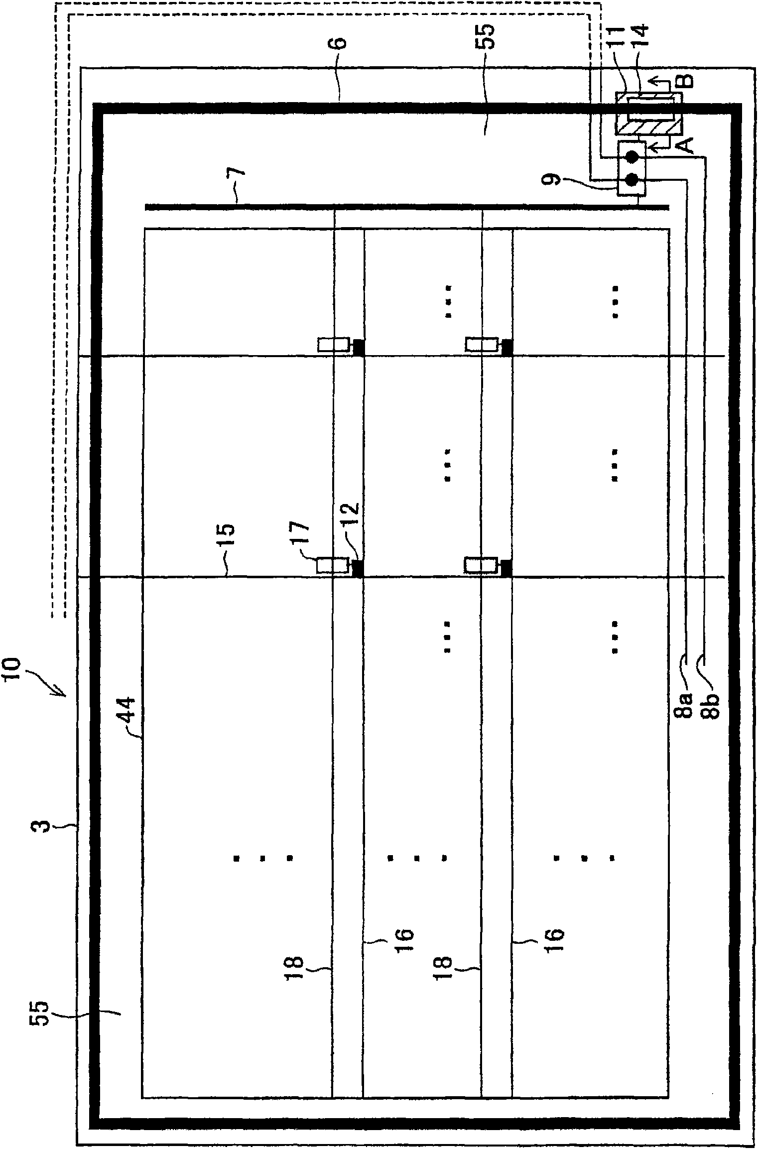
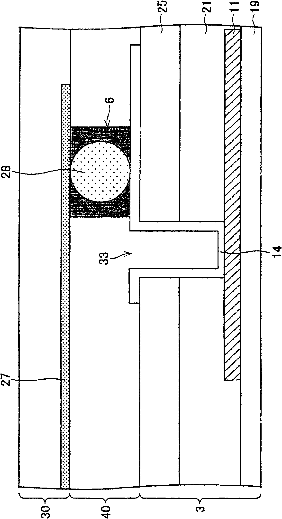
[0062] figure 1 It is a plan view showing the structure of this liquid crystal panel, figure 2 yes figure 1 A-B cross-sectional view.

[0063] Such as figure 1 , 2 As shown, the liquid crystal panel 10 includes: an active matrix substrate 3, a color filter substrate 30, a liquid crystal material 40 arranged between the two substrates (3, 30), and a liquid crystal material 40 for bonding the two substrates and encapsulating the liquid crystal material 40. The sealing member 6 between the two substrates.

[0064] The active matrix substrate 3 includes a plurality of scanning signal lines 16 and a plurality of data signal lines 15 arranged to intersect, TFTs 12 (switching elements) formed near intersections of the respective signal lines ( 15 , 16 ), and pixel electrodes 17 . Among them, the gate electrode of the TFT 12 is connected to the scanning signal line 1...


PUM


Abstract

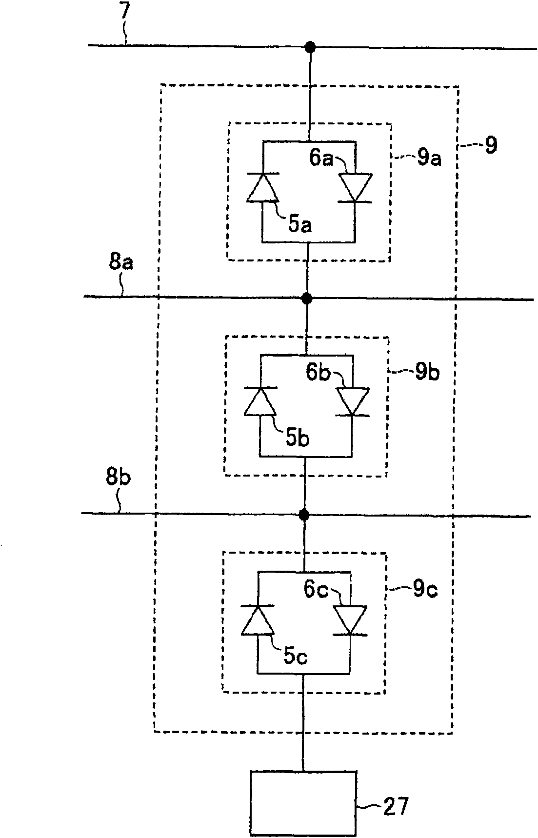
A liquid crystal panel (10) is provided with an active matrix substrate whereupon a transistor (12), a pixel electrode (17), signal lines (15, 16) and backup wirings (8a, 8b) for modifying defects of the signal lines are formed; a color filter substrate whereupon a common electrode (counter electrode) is formed; and a liquid crystal material arranged between the both substrates. The backup wirings (8a, 8b) are (electrically) connected to the common electrode on the color filter substrate, through a protection circuit (9) for releasing undesired charges generated on the backup wirings (8a, 8b) and a seal (6). Problems (for instance, unexpected short-circuit of the backup wirings and the signal line) due to the undesired charges generated on the backup wirings can be reduced.

Description

technical field [0001] The present invention relates to spare wiring provided on a liquid crystal panel. Background technique [0002] Figure 9 It is a plan view showing the structure of a conventional liquid crystal panel. As shown in this figure, the liquid crystal panel 110 includes: an active matrix substrate 103, a color filter substrate (not shown), a sealing member 106 for bonding these two substrates, and a filling area surrounded by the two substrates and the sealing member 106. The liquid crystal material (not shown) in the part. [0003] The active matrix substrate 103 includes: a plurality of scanning signal lines 116 and a plurality of data signal lines 115 arranged crosswise, a TFT 112 (Thin Film Transistor: thin film transistor) formed near the intersection of each signal line (115, 116), and pixel electrode 117 . Among them, regarding the TFT 112 , its gate electrode is connected to the scanning signal line 116 , its source electrode is connected to the d...

Claims


Application Information

Patent Timeline
Patent Type & Authority Applications(China)
IPC IPC(8): G02F1/1343G02F1/1345G02F1/1368H04N5/66
CPCG02F1/136259G02F1/136204G02F2001/136272G02F1/136272
Inventor 松田成裕武内正典
Owner SHARP KK
Learn More