Solar cell silicon chip detecting system

A technology of solar cells and detection systems, applied in the field of detection systems, can solve the problems of increased probability, detection time, cost, undetectable, sorting, etc., and achieve the effect of easy operation

Active Publication Date: 2009-11-18
武汉中导光电设备有限公司
View PDF0 Cites 49 Cited by
  • Summary
  • Abstract
  • Description
  • Claims
  • Application Information

AI Technical Summary

Problems solved by technology

However, the existing solar cell silicon wafer inspection system cannot complete the inspection and sorting on one conveying device, which increases the probability of defects, inspection time and cost

Method used


Image

  • Solar cell silicon chip detecting system
  • Solar cell silicon chip detecting system
  • Solar cell silicon chip detecting system

Examples


Embodiment 1

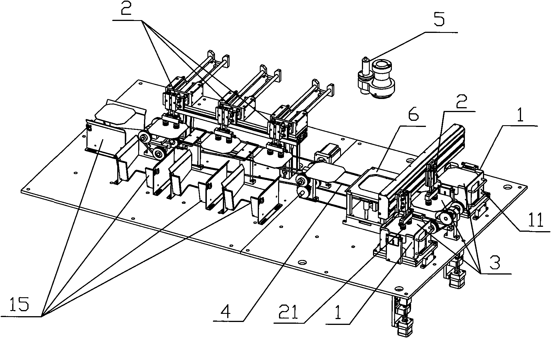
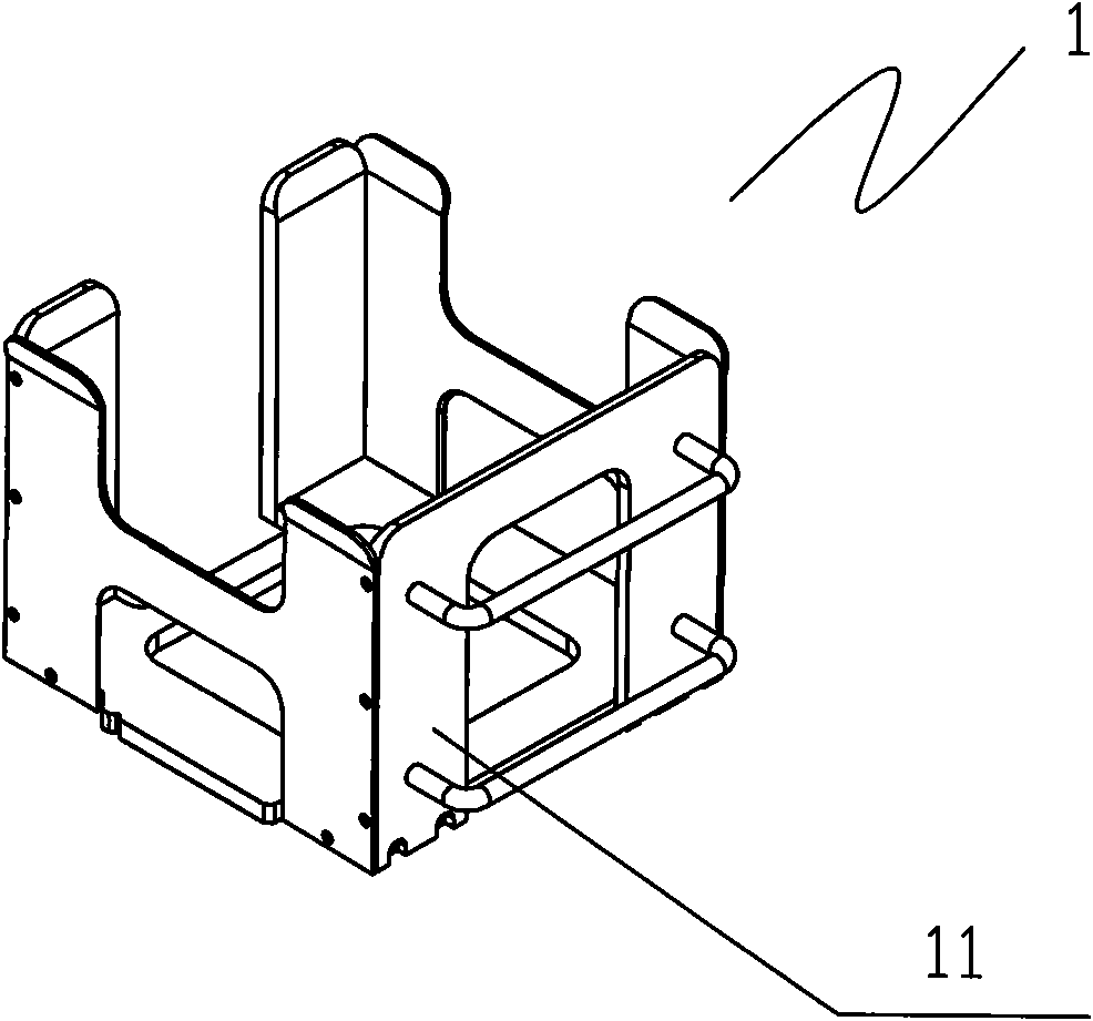
[0043] figure 1 It is a schematic diagram of a silicon wafer detection system for solar cells using the principle of photoluminescence according to the present invention. From right to left in the figure, along the silicon wafer conveyor belt, there are feeding area, exposure area, inspection waiting area, and sorting area. The area includes a loading box 1 and a manipulator 2. The front panels 11 of the two loading boxes 1 can be opened around the shaft at the bottom of the loading box 1, and the silicon wafer 3 can be placed in the loading box 1 by hand (such as figure 2 ), the manipulator 2 extracts the silicon wafer 3 through the suction cup 21 and puts it on the conveyor belt 4. After the silicon wafer 3 is placed on the conveyor belt 4, it is known to the electric control and UI, and the silicon wafer 3 is transported to the exposure area through the conveyor belt 4.

[0044] The exposure area is provided with an illumination system, an imaging system 5 and a photofluor...

Embodiment 2

[0052] The difference between embodiment 2 and embodiment 1 is that electroluminescence is used to expose and image the silicon wafer, and an electroluminescence limit mechanism is designed according to the principle of electrofluorescence. The imaging system no longer needs an illumination system. 1 is basically the same.

[0053] The principle of embodiment 2 is to cause the silicon wafer to emit light by applying current to the silicon wafer of the solar cell, and the quality of the silicon wafer can be judged according to the luminous intensity. The photoluminescent detection method can be used for all process detection after the PN junction is formed, while the electroluminescent detection method can only be used after screen printing.

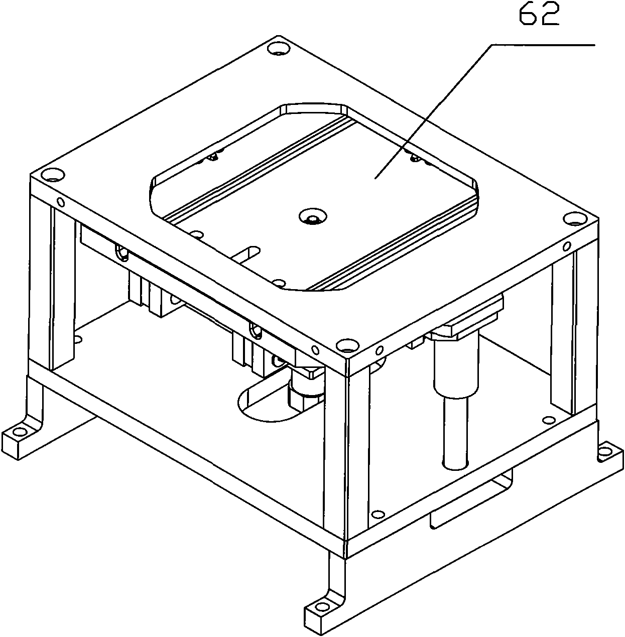
[0054] Figure 12 It is a schematic diagram of the electroluminescence solar cell silicon wafer detection system of embodiment 2, and the photoluminescent limiting mechanism 6 is different in that the electroluminescent limiting mechanis...


PUM


Abstract

The invention relates to a detecting system, in particular to a solar cell silicon chip detecting system. The detecting system comprises a silicon chip conveying device; the silicon chip conveying device is provided with a feeding area, an exposure area and a sorting area along the silicon chip conveying device in sequence; the feeding area is used for arranging the silicon chips on the silicon chip conveying device; the exposure area is provided with a detecting and imaging system arranged above the silicon chips and a limiting mechanism used for limiting the silicon chips; and the sorting area is used for putting the silicon chips with different weight into corresponding material-receiving box. Compared with the prior art, the system has the beneficial effects that by adopting the structure, the detecting system can realize sorting to the silicon chips by only needing arranging the silicon chips into a feeding box of the feeding area, and is simple and practical.

Description

technical field [0001] The invention relates to a detection system, in particular to a solar cell silicon wafer detection system. Background technique [0002] The main components of solar panels are solar silicon wafers. The photoelectric conversion efficiency of solar silicon wafers has been continuously improved. It has extremely important applications in civil, national defense, aviation, aerospace and other aspects, and has become an indispensable member of clean energy. One, the industry has a strong demand for solar silicon wafers. Due to the thinness of solar silicon wafers, in the automatic manufacturing and testing process, if there is a slight carelessness, it may cause damage, missing corners or even tiny cracks that cannot be observed by the naked eye. These defects should be avoided as much as possible to improve the quality of solar panels. However, the existing inspection system for silicon wafers of solar cells cannot complete the inspection and sorting on ...

Claims


Application Information

Patent Timeline
Patent Type & Authority Applications(China)
IPC IPC(8): G01N21/64G01N21/88B07C5/342
Inventor 裴世铀李波杨铁成樊思民陈利平
Owner 武汉中导光电设备有限公司
Why Eureka
Try Eureka