Embedded intelligent card matrix and manufacturing method thereof
A smart card base and manufacturing method technology, which is applied to recording carriers used in machines, instruments, computer parts, etc., can solve problems such as not meeting energy saving requirements and high energy consumption, and achieve easy control of product size, energy saving, and improved efficiency effect
- Summary
- Abstract
- Description
- Claims
- Application Information
AI Technical Summary
Problems solved by technology
Method used
Image
Examples
Embodiment 1
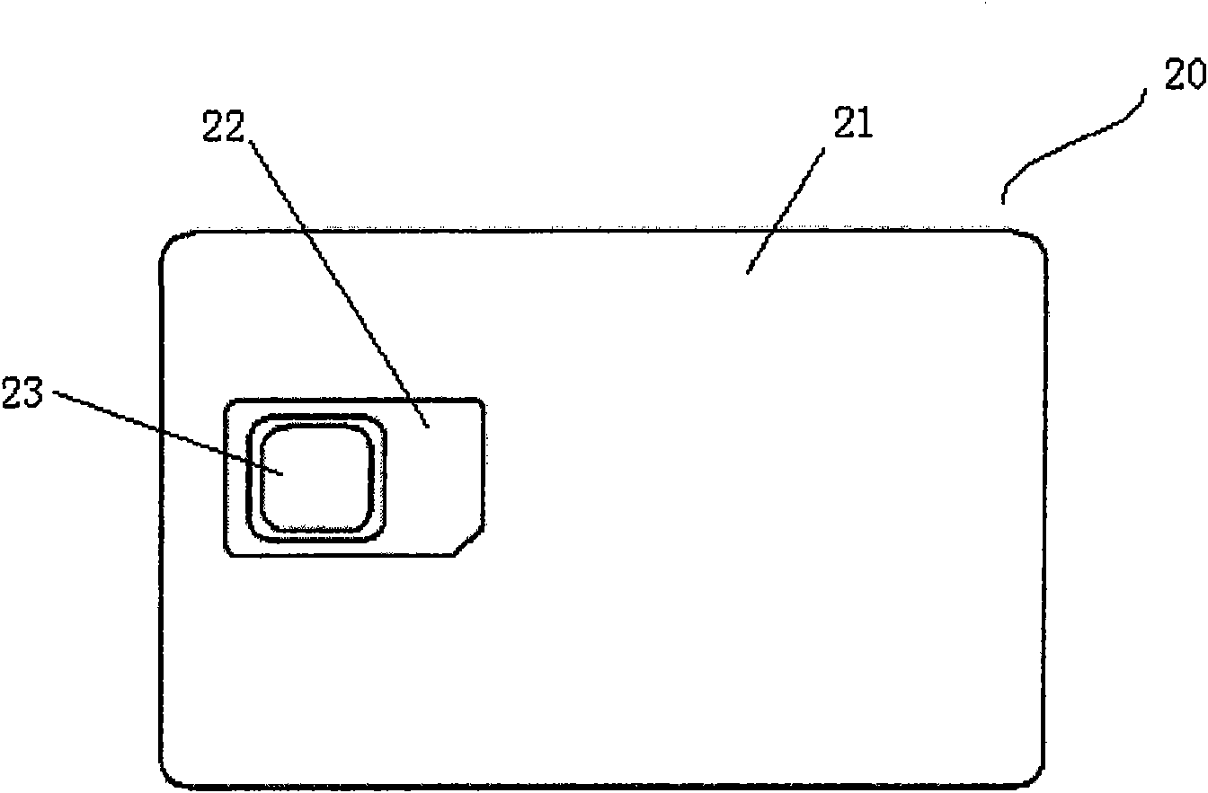
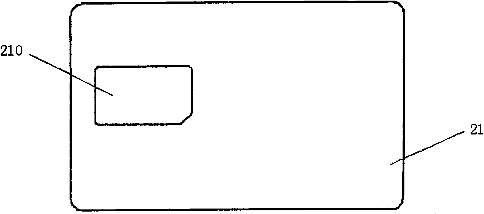
[0059] image 3 It is a structural schematic diagram of the mother card base of the mosaic smart card base of the present invention; Figure 4 It is an exploded schematic diagram of an embodiment of the mother card base of the embedded smart card base of the present invention; Figure 5 It is a three-dimensional schematic diagram of the mother card base structure of the mosaic smart card base of the present invention; Figure 5A Yes Figure 5 A partially enlarged schematic diagram. like image 3 , Figure 4 , Figure 5 , Figure 5A shown, and please also refer to the figure 2 , The mosaic smart card base 20 of the present invention includes a mother card base 21 and a small card base 22 arranged in the mother card base 21 and capable of being separated. The mother card base 21 is composed of more than one layer of paper base, and at least one packaging hole 210 is arranged on it. The small card base 22 is made of a high molecular polymer material, and its shape match...
Embodiment 2
[0082] Figure 6A It is a schematic front view of an embodiment of the small card base of the embedded smart card base of the present invention; Figure 6B Yes Figure 6A The schematic diagram of the top view; Figure 6C Yes Figure 6A side view diagram of Figure 6D Yes Figure 6C Partial enlarged schematic diagram of ; Figure 6E It is a schematic diagram of the small card base structure after partial sectioning.
[0083] like Figure 6A , Figure 6B , Figure 6C , Figure 6D and Figure 6E As shown, the difference between this embodiment and the above-mentioned embodiment 1 is mainly that, on the connection surface 220 connected with the outer periphery of the small card base 22 and the female card base 21, there is a middle part with the female card base 21. The grooves 221, 222 corresponding to the glue overflow port 2122 provided on the layer 212 can be embedded in the grooves 221, 222 after the hot melt glue in the pre-embedded capsule of the mother card base...
Embodiment 3
[0088] Figure 7 It is a structural schematic diagram of another embodiment of the mother card base of the mosaic smart card base of the present invention; Figure 8 It is a structural schematic diagram of another embodiment of the small card base of the embedded smart card base of the present invention; Figure 9 It is a schematic structural view of the small card base of the present invention embedded in the mother card base.
[0089] like Figure 7 , 8 , 9, the difference between this embodiment and the above-mentioned embodiment 1 is that at least one of the main card base 31 or the small card base 32 is provided with glue injection gaps 311, 321 on the top or bottom. In the illustration of this embodiment, only the situation where the glue injection gap is provided on the lower surface is shown.
[0090] like Figure 7 As shown, the glue injection gap can be provided only on one side of the mother card base 31, on the side of the packaging hole 310, and make one side...
PUM
 Abstract
Description
Claims
Application Information


