Thin film transistor (TFT) array substrate and manufacture method thereof

A technology for thin film transistors and array substrates, applied in the field of thin film transistor array substrates and their manufacturing, can solve the problem that the gate insulating layer cannot fully meet the design requirements, and achieves reduction in the number of photomasks, high stability, and improved resistance. delay-tolerant effect

Active Publication Date: 2009-11-18
AU OPTRONICS CORP
View PDF0 Cites 5 Cited by
  • Summary
  • Abstract
  • Description
  • Claims
  • Application Information

AI Technical Summary

Problems solved by technology

Therefore, the gate insulating layer with the same dielectric constant in different regions cannot fully meet the design requirements.

Method used


Image

  • Thin film transistor (TFT) array substrate and manufacture method thereof
  • Thin film transistor (TFT) array substrate and manufacture method thereof
  • Thin film transistor (TFT) array substrate and manufacture method thereof

Examples


Embodiment Construction

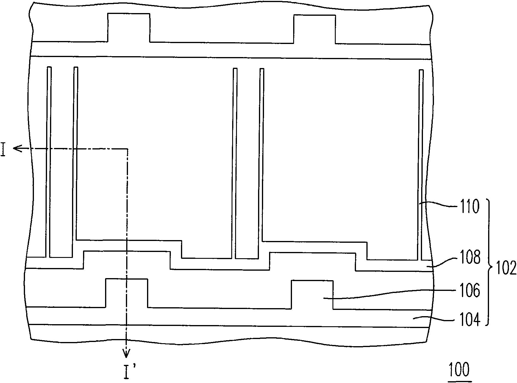
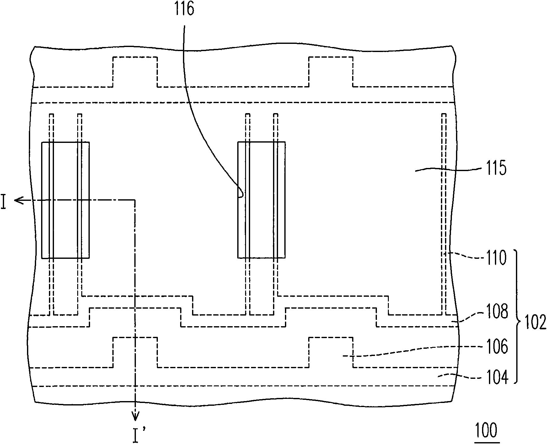
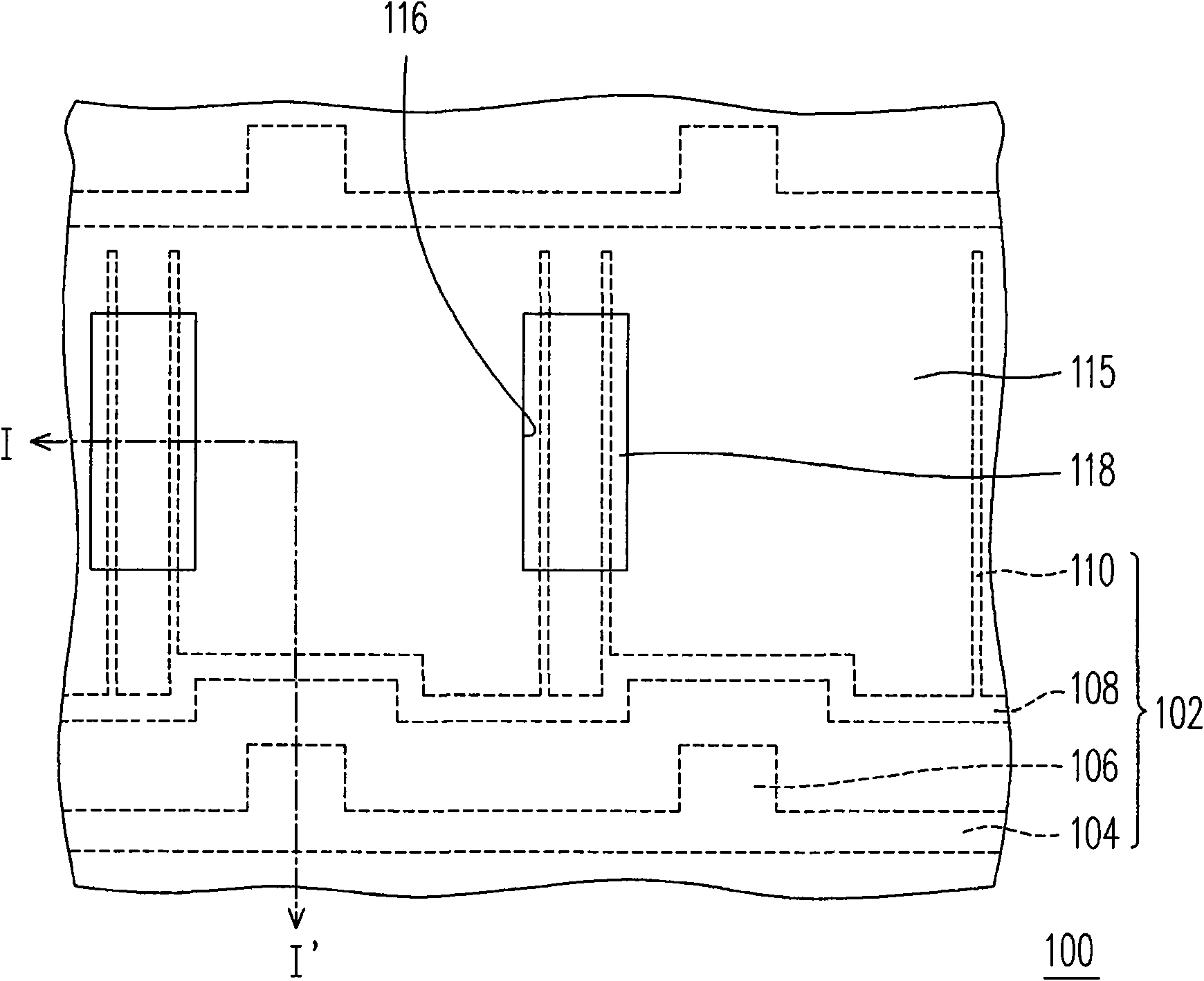
[0059] Figure 1A to Figure 1E It is a schematic top view of a thin film transistor array substrate according to an embodiment of the present invention. Figure 2A to Figure 2E respectively according to Figure 1A to Figure 1E The schematic cross-sectional view of the thin film transistor array substrate shown in the I-I' cross-section in . First, please also refer to Figure 1A and Figure 2A , forming a patterned conductive layer 102 on the substrate 100 . The material of the substrate 100 is, for example, glass, plastic or other suitable materials. The material of the patterned conductive layer 102 is, for example, metal. The patterned conductive layer 102 includes a scan line 104 and a gate 106 connected to the scan line 104 . In addition, the patterned conductive layer 102 also includes a common line 108 . A part of the common line 108 serves as a shielding layer 110 , for example, the shielding layer 110 can be parallel to the data line 124 .

[0060] Then, please ...


PUM


Abstract

The invention relates to a TFT array substrate and a manufacture method thereof. The method includes the steps of first forming a first patterned conducting layer comprising a plurality of scanning lines and a plurality of grid electrodes connected with the scanning lines on the substrate; then forming a patterned grid insulating layer with a plurality of open pores on the substrate so as to cover the first patterned conducting layer and forming a plurality of dielectric patterns in the open pores; subsequently, forming a plurality of semiconductor patterns on the patterned grid insulating layer; after that, forming a second patterned conducting layer on the semiconductor patterns, the patterned grid insulating layer and the dielectric patterns; then forming a protective layer on the semiconductor patterns, the patterned grid insulating layer and the dielectric patterns; and finally forming a plurality of pixel electrodes on the protective layer. The invention can decrease the number of driving elements to achieve the purpose of reducing cost, simultaneously integrate the characteristic stability and high storage capacitance value of the TFT elements to satisfy the requirements on the design of the elements, and also achieve the effect of lessening the number of photo masks.

Description

technical field [0001] The invention relates to a thin film transistor array substrate and a manufacturing method thereof, and in particular to a thin film transistor array substrate capable of improving resistance-capacitance delay (RC delay) and a manufacturing method thereof. Background technique [0002] With the advancement of display technology, people can make their lives more convenient with the assistance of displays. In order to achieve the characteristics of lightness and thinness of displays, flat panel displays (FPDs) have become the current mainstream. Among many flat panel displays, a liquid crystal display (LCD) has superior characteristics such as high space utilization efficiency, low power consumption, no radiation, and low electromagnetic interference. Therefore, the liquid crystal display is very popular among consumers. [0003] A liquid crystal display is mainly composed of an active matrix substrate, a color filter substrate and a liquid crystal layer...

Claims


Application Information

Patent Timeline
Patent Type & Authority Applications(China)
IPC IPC(8): H01L27/12H01L23/532H01L21/84H01L21/768G02F1/1368
Inventor 陈建宏詹立雄廖金阅曾贤楷
Owner AU OPTRONICS CORP
Why Eureka
Try Eureka