Unlock instant, AI-driven research and patent intelligence for your innovation.

Image sensor module package structure with supporting element

An image sensing and packaging structure technology, applied in the direction of electrical components, electric solid devices, semiconductor devices, etc., can solve the problem that the image sensing module packaging structure 10 cannot accurately and sensitively sense images, and general products do not have suitable structures , Impossible to correctly sense the image and other problems, to achieve the effect of improving the yield of production, improving the accuracy and sensitivity, and widely using value

Inactive Publication Date: 2009-11-18
KINGPAK TECH INC
View PDF1 Cites 16 Cited by
  • Summary
  • Abstract
  • Description
  • Claims
  • Application Information

AI Technical Summary

Problems solved by technology

[0009] However, since only the transparent layer 11 is bonded to the chip 13 through the colloidal layer 12, there is only a very short distance between the transparent layer 11 and the photosensitive element 14, so imaging aberrations are likely to occur, thereby causing The light sensing element 14 cannot correctly sense the image
In addition, if there are defects or blemishes on the light-transmitting layer 11, they will be directly amplified, so that the image sensing module packaging structure 10 cannot accurately and sensitively sense images.
[0010] It can be seen that the above-mentioned existing image sensor module packaging structure obviously still has inconvenience and defects in structure and use, and needs to be further improved urgently.
In order to solve the above-mentioned problems, the relevant manufacturers have tried their best to find a solution, but no suitable design has been developed for a long time, and the general products do not have a suitable structure to solve the above-mentioned problems. Urgent problem

Method used


Image

  • Image sensor module package structure with supporting element
  • Image sensor module package structure with supporting element
  • Image sensor module package structure with supporting element

Examples


Embodiment Construction

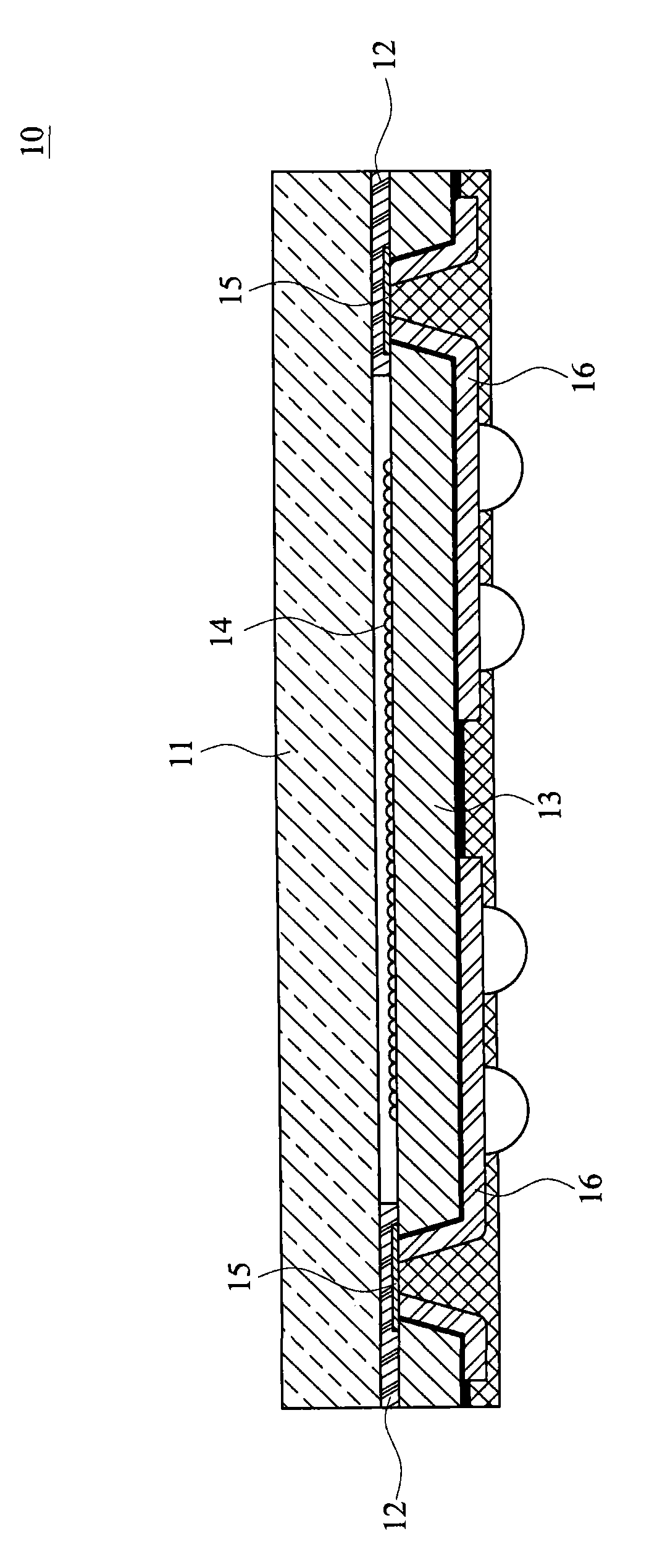
[0060] In order to further explain the technical means and effects adopted by the present invention to achieve the intended purpose of the invention, the specific implementation of the image sensing module packaging structure with supports proposed according to the present invention will be described below in conjunction with the accompanying drawings and preferred embodiments. , structure, feature and effect thereof, detailed description is as follows.

[0061] The aforementioned and other technical contents, features and effects of the present invention will be clearly presented in the following detailed description of preferred embodiments with reference to the drawings. Through the description of the specific implementation mode, when the technical means and functions adopted by the present invention to achieve the predetermined purpose can be obtained a deeper and more specific understanding, but the accompanying drawings are only for reference and description, and are not...


PUM


Abstract

An image sensor module package structure with a supporting element comprises a chip, the supporting element and a light-transmitting element. The chip has light-sensing elements arranged on a light-sensing area of a first surface thereof, first conducting pads electrically connected to the light-sensing elements, and a conducting channel passing through the chip and electrically connected to the first conducting pads at one end. The supporting element has an opening, a first coupling surface, and a second coupling surface. The opening corresponds to the light-sensing area and the first coupling surface is combined with the first surface of the chip while the light-transmitting element is combined with the second coupling surface. The supporting element separates the light-transmitting element from the chip by a proper distance, so as to enhance an image sensing accuracy of an image sensor module. The chip having the conducting channel effectively facilitates reducing an overall volume of the image sensor module package structure.

Description

technical field [0001] The present invention relates to an image sensing module packaging structure with a support, in particular to an image sensing module packaging structure that can improve the accuracy and sensitivity of image sensing, save wiring space, and can Reducing the packaging volume of the image sensing module packaging structure can also improve the production yield of the image sensing module packaging structure. The image sensing module packaging structure has a support. Background technique [0002] With the advent and popularization of various digital imaging products, the demand for image sensing modules used in digital imaging products such as digital cameras, mobile cameras, video phones, fingerprint readers, etc. is gradually increasing. . Generally speaking, according to the different light sensing elements used in the image sensing module, it can be mainly divided into a complementary metal oxide semiconductor image sensing module and a charge-coupl...

Claims


Application Information

Patent Timeline
Patent Type & Authority Applications(China)
IPC IPC(8): H01L27/146
CPCH01L27/14685H01L27/14618H01L2224/13H01L2224/05024H01L2224/05022H01L2224/05548H01L2224/05001H01L2924/00014H01L24/02H01L2224/02377H01L2224/13024H01L2224/02372H01L2224/05599H01L2224/05099H01L27/146
Inventor 辛宗宪庄俊华彭镇滨张建伟林建亨
Owner KINGPAK TECH INC