Failure testing system for embedded logic cores in system on chip

A technology of logic core and system-on-chip, applied in the field of integrated circuit fault test system

Inactive Publication Date: 2009-11-25
SHANGHAI UNIV
View PDF0 Cites 15 Cited by
  • Summary
  • Abstract
  • Description
  • Claims
  • Application Information

AI Technical Summary

Problems solved by technology

However, it must be noted that this standard only has a relatively complete design definition for the function and behavior of the test ring, and only gives a framework definition for the te

Method used


Image

  • Failure testing system for embedded logic cores in system on chip
  • Failure testing system for embedded logic cores in system on chip
  • Failure testing system for embedded logic cores in system on chip

Examples


Embodiment Construction

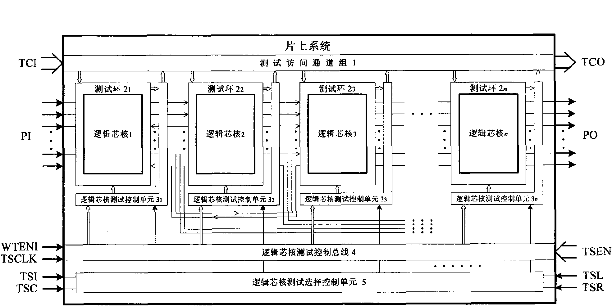
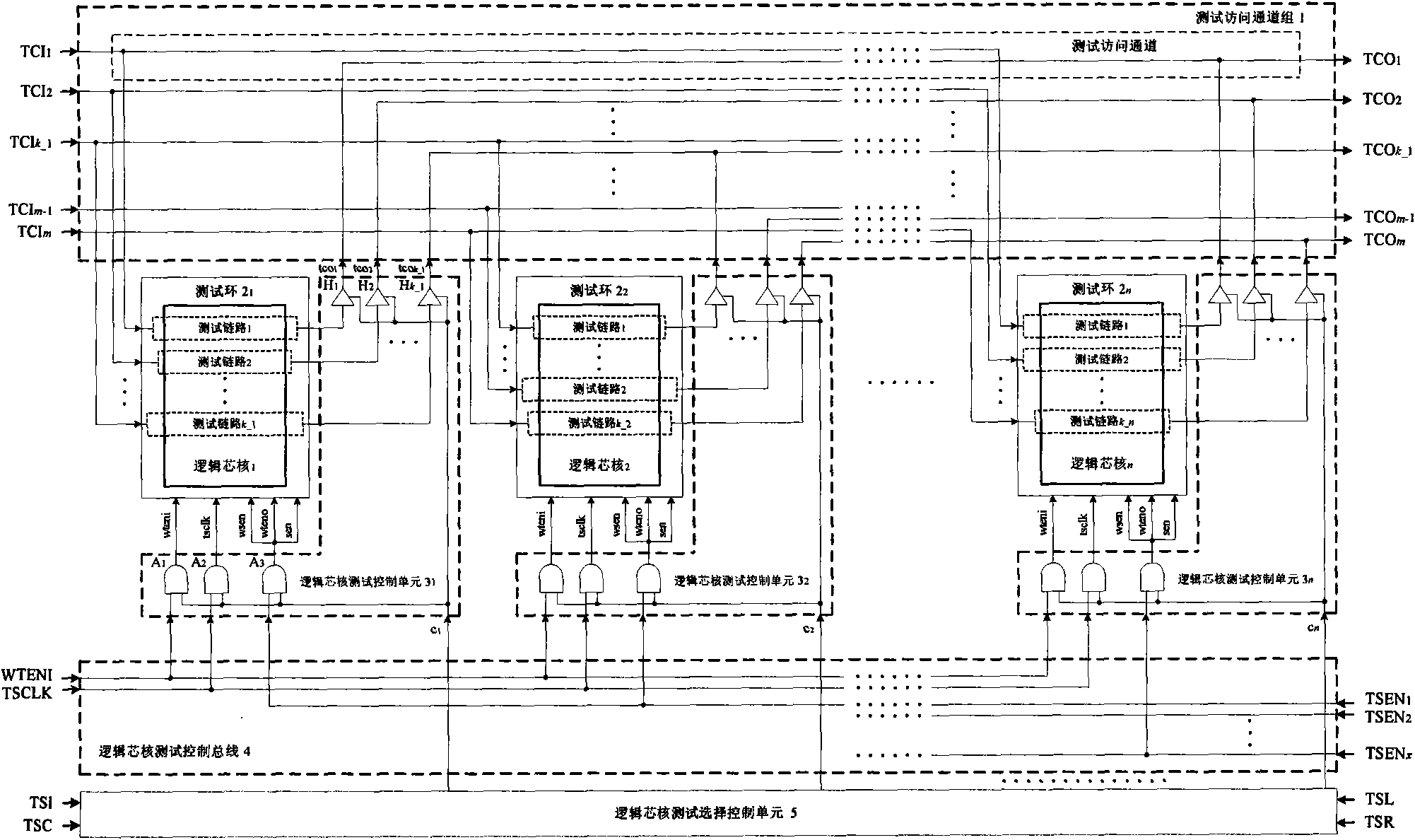
[0034] A preferred embodiment of the present invention is: see figure 1 , the fault test system of the embedded logic core in the SoC is a circuit added to improve the fault test of the embedded logic core. Its circuit consists of a test access channel group 1, n test rings 2, n logic core test control units 3, a logic core test control bus 4 and a logic core test selection control unit 5, where n is the system on chip The number of logical cores in .

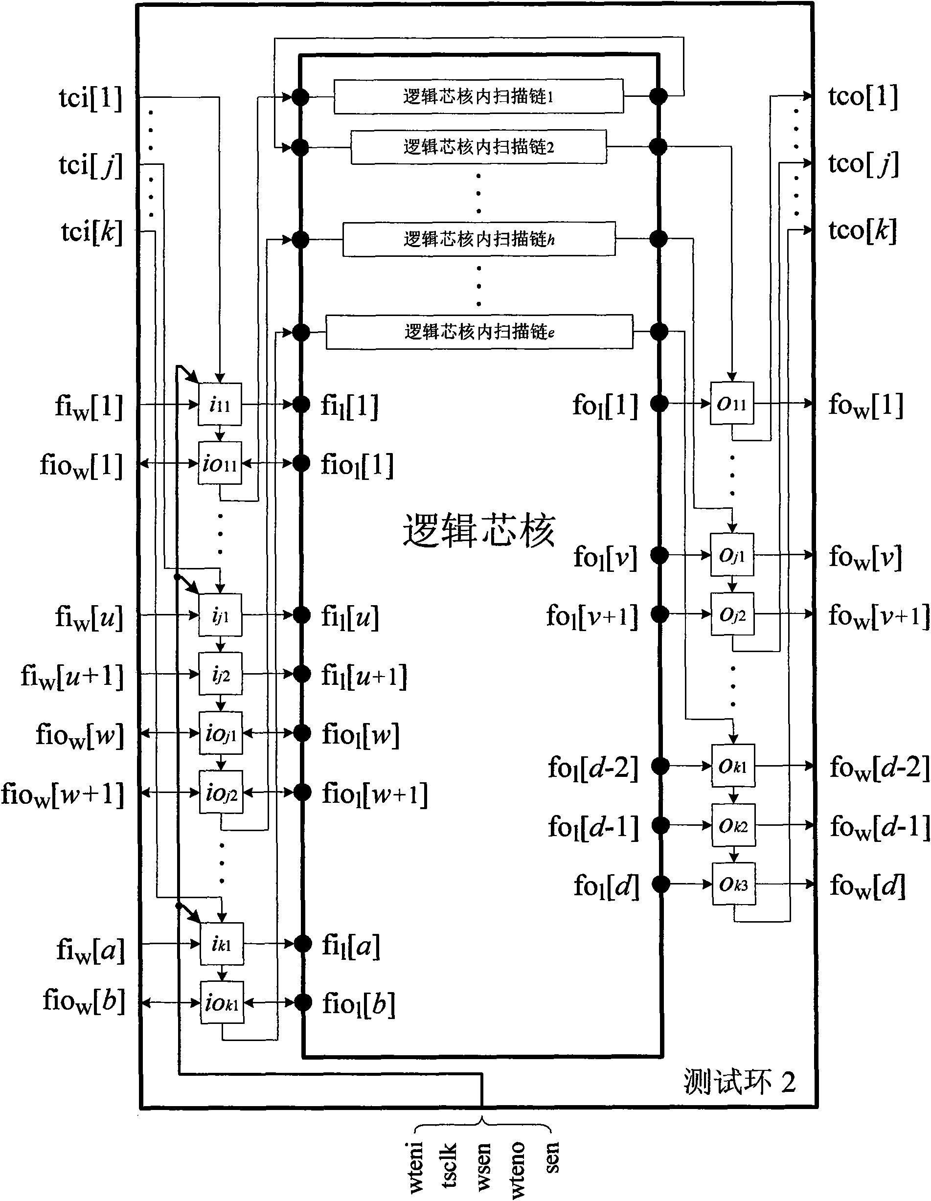
[0035] This circuit structure is: see figure 1 , the test access channel group 1 has a set of external test access channel signal input pins TCI and a set of external access test channel signal output pins TCO, and the on-chip output test ring 2 connected to each logic core; each test ring 2 There is a group of external system-on-chip function signal input pins PI or system-on-chip function signal output pins PO, and the internal logic core and output connections are connected to the logic core test control unit 3 and other t...


PUM


Abstract

The invention relates to a failure testing system for embedded logic cores in a system on chip, which is a circuit added for perfecting testability of the system on chip. The circuit thereof is composed of a testing access channel set, n testing loops, n logic core testing control units, a logic core testing control bus and a logic core testing selection control unit, wherein n is number of the logic cores in the system on chip. The invention can comprehensively test and access each deeply embedded logic core in the system on chip, and can guarantee mutual separation and effective control of each logic core in testing process. The circuit has simple structure and is applied to various systems on chip constructed by using embedded logic core design method.

Description

technical field [0001] The invention relates to a fault testing system for an integrated circuit, in particular to a fault testing system which can be repeatedly applied to a SOC System on a Chip (SOCSystem on a Chip) integrated circuit. Background technique [0002] Advanced semiconductor processing and design techniques have greatly increased the likelihood of successful integrated circuit design for complex systems. The traditional design method based on the standard cell library is gradually replaced by a design method using a larger-scale reusable logic core (IntellectualProperty Core). Due to the use of logic core reuse design methods, the design scale and implementation functions of integrated circuits have undergone a sudden change, from the original VLSI (Very Large Scale Integration Circuit) to the current system-on-chip. However, with the increasing design scale, increasing functional complexity and shortening design cycle of SoC, a serious problem is becoming mo...

Claims


Application Information

Patent Timeline
IPC IPC(8): G01R31/28G01R31/317
Inventor 张金艺李娇王佳翁寒一蔡万林张冬杨晓冬施慧黄徐辉杨毅
Owner SHANGHAI UNIV
Why Eureka
Try Eureka