

Capacitance touch screen and method for preparing the same
A technology of capacitive touch screen and manufacturing method, which is applied in the direction of electric digital data processing, instrument, input/output process of data processing, etc., and can solve the problem of high wire resistance of conductive film, low sensitivity and resolution, wire breakage, etc. problem, to achieve the effect of improving the yield rate, improving sensitivity and resolution, and eliminating electrical interference
- Summary
- Abstract
- Description
- Claims
- Application Information
AI Technical Summary
Problems solved by technology
Method used
Image

Examples
Embodiment Construction
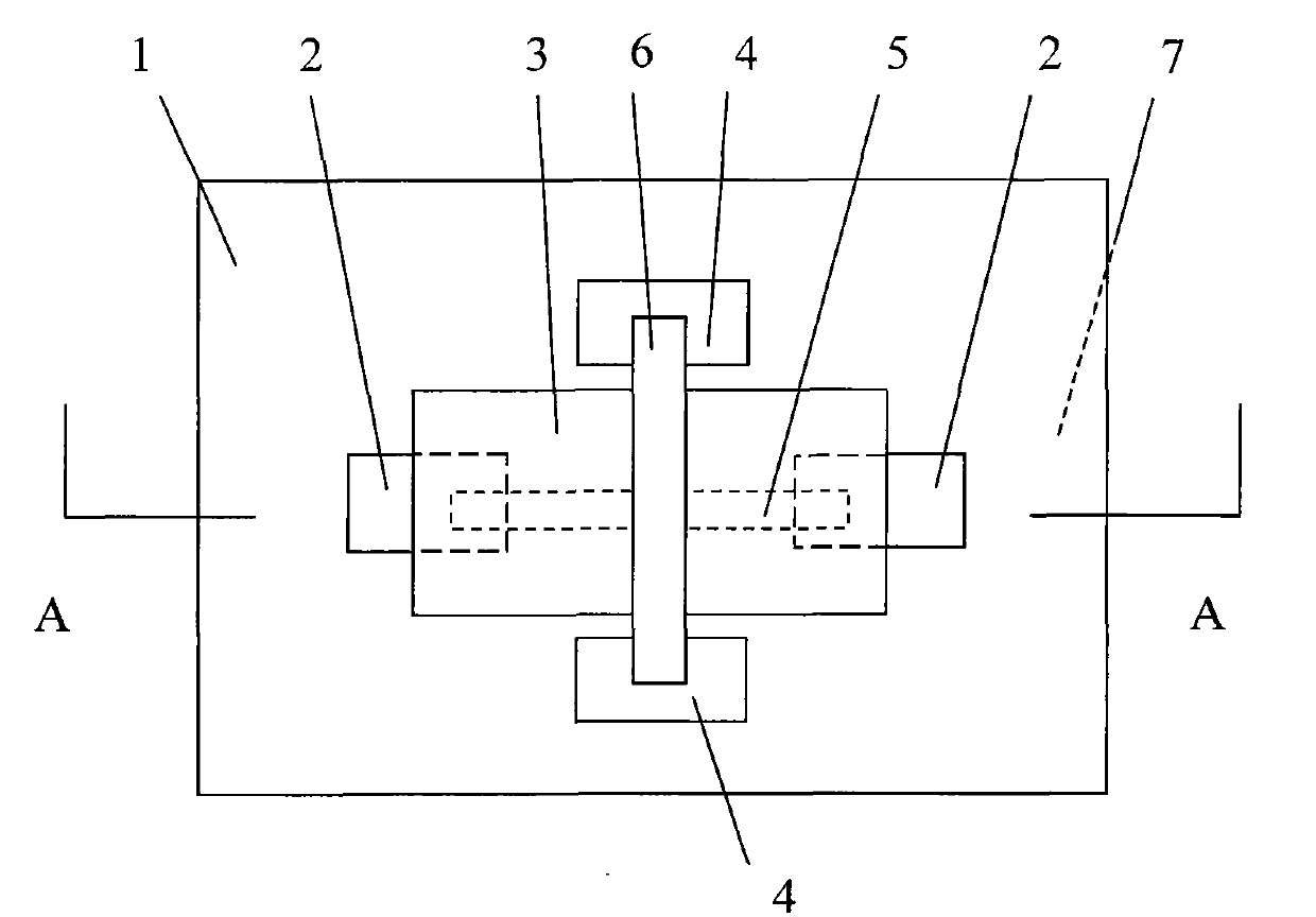
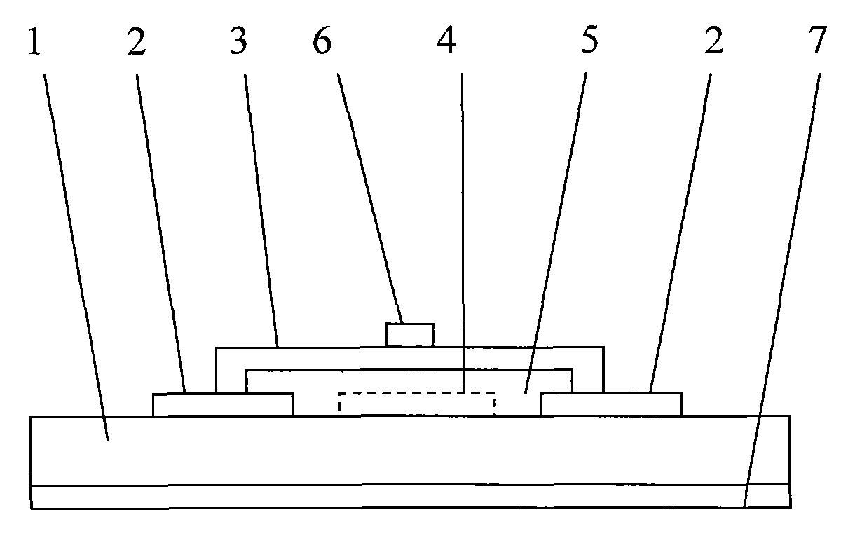
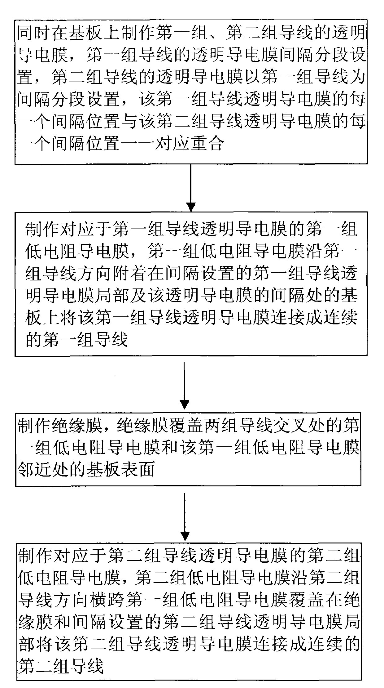
[0036] like figure 1 , figure 2 As shown, the capacitive touch screen of the present invention includes a substrate 1 , two sets of transparent conductive films of wires arranged on the substrate 1 along X and Y directions, an insulating film 3 and two sets of low-resistance conductive films.
[0037] The transparent conductive film 2 of the first group of wires in the two groups of wires is arranged in intervals and segments, and the transparent conductive film 4 of the second group of wires is arranged in segments at intervals of the first group of wires. Each of the transparent conductive films 2 of the first group of wires A spacing position coincides with each spacing position of the transparent conductive film 4 of the second group of wires in a one-to-one correspondence.
[0038] The first group of low-resistance conductive films 5 in the two groups of low-resistance conductive films are arranged corresponding to the first group of conductive transparent conductive fi...
PUM
 Abstract
Description
Claims
Application Information