Quasi-one-dimensional metal oxide nano-material biosensor and method for manufacturing same
A biosensor and nanomaterial technology, applied in the field of quasi-one-dimensional metal oxide nanomaterial biosensors and their fabrication, can solve long-term problems, often requiring more than a few hours, a certain number of samples, and the sensitivity needs to be improved. , to achieve the effect of improving sensitivity and detection speed, wide application range, and shortening sample preparation and processing time
- Summary
- Abstract
- Description
- Claims
- Application Information
AI Technical Summary
Benefits of technology
Problems solved by technology
Method used
Image
Examples
Embodiment 1
[0059] Combination with DNA or RNA probes to detect viral diseases, such as Image 6 ; Specific process such as Figure 2 to Figure 5 .
[0060] Preparation of quasi-one-dimensional metal oxide semiconductor nanomaterials and device fabrication:
[0061] Synthesis of TiO by Solvothermal Method 2 and ZnO nanomaterials, take a certain proportion of reactants, stir rapidly, and react in an autoclave for 16-24 hours after cleaning.
[0062] Based on the VLS (gas-liquid-solid) growth mechanism, nanowires (ZnO or TiO 2 ), the length of the nanowire is controlled by controlling the gas flow rate, air pressure, and growth time, and the specific steps are as follows:
[0063] 1. Deposit a layer of Au film of about 1-10nm on the Si substrate by electron beam evaporation;
[0064] 2. Sprinkle 325-mesh Zn powder (99.999%) evenly on the quartz boat, and place the Si substrate deposited with the Au film upside down on the quartz boat;
[0065] 3. Turn on the mechanical pump and the mo...
Embodiment 2
[0084] Rapid diagnosis of myocardial infarction and acute pancreatitis, such as Figure 7 , the specific process is as Figure 2 to Figure 5 .
[0085] Preparation of quasi-one-dimensional metal oxide semiconductor nanomaterials and device fabrication:
[0086] Synthesis of TiO by Solvothermal Method 2 And ZnO nanomaterials. Take a certain proportion of reactants, stir rapidly, and react in an autoclave for 16-24 hours after cleaning.
[0087] The standard process of micro-nano photolithography is used to fabricate the contact electrodes of oxide nanomaterials.
[0088] Fabrication process and integration of quasi-one-dimensional metal oxide nanomaterial devices:
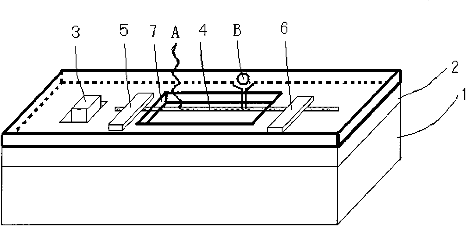
[0089] 1. Silica growth, such as figure 2 Shown; clean the silicon wafer, and form a silicon dioxide oxide layer 2 with a thickness of 100-400 nanometers on the surface of the silicon wafer 1 by thermal growth.
[0090] 2. Fabrication of the back gate, such as image 3 As shown; the position of the back gat...
PUM
| Property | Measurement | Unit |
|---|---|---|
| Thickness | aaaaa | aaaaa |
Abstract
Description
Claims
Application Information


