Method for producing metal electrode of front panel of shadow mask plasma display panel capable of preventing panel from yellowing
A plasma and display panel technology, applied in electrode system manufacturing, discharge tube/lamp manufacturing, cold cathode manufacturing, etc., can solve the problems of low production efficiency, large waste of resources, low picture quality, etc., to improve production efficiency , to eliminate waste, to reduce the effect of speed
- Summary
- Abstract
- Description
- Claims
- Application Information
AI Technical Summary
Problems solved by technology
Method used
Image

Examples
Embodiment 1
[0036] Such as Figure 1-5 shown.
[0037] A method for manufacturing a metal electrode on the front plate of a shadow mask type plasma display panel that can prevent yellowing of the panel. A black paste layer that does not contain silver, and then form a conductive silver paste on the black paste layer to prepare electrodes to prevent the replacement reaction between the silver ions in the conductive silver paste and the Na and K metal ions in the glass substrate to cause yellowing of the panel occurrence of the phenomenon.
[0038] The specific production steps include:
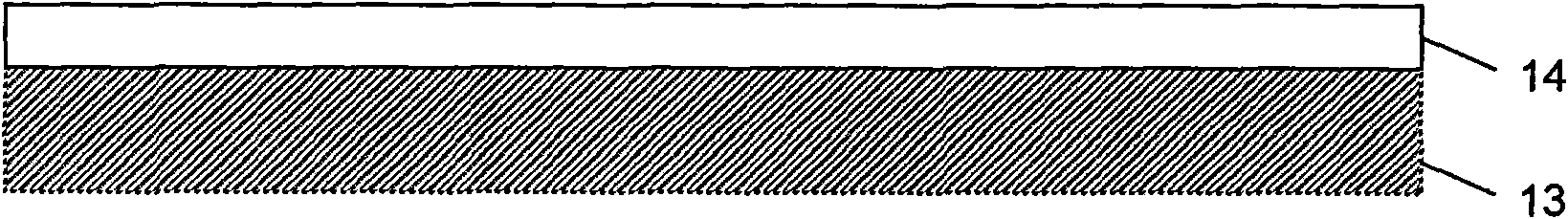
[0039] a. clean the glass substrate 13 (can be the glass substrate that finally forms the front substrate glass substrate 8, also can be the glass substrate that finally forms the rear substrate glass substrate 4), make PVA on the surface of the glass substrate 13, and can be burned The photosensitive layer 14 decomposed in the forming process, the thickness of the photosensitive layer 14 is controlled ...
example 1
[0049] A method for making a front plate metal electrode specifically comprises the following steps:
[0050] 1. Clean the glass substrate 13, and form a photosensitive layer 14 with a thickness of 10-30 μm on the surface of the glass substrate 13.
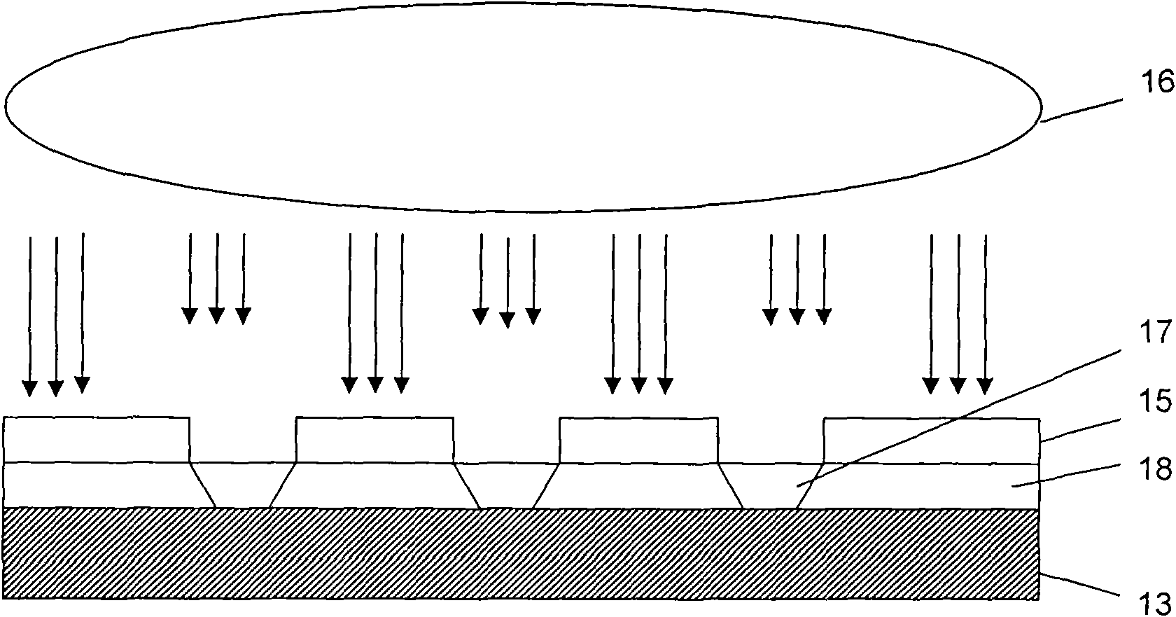
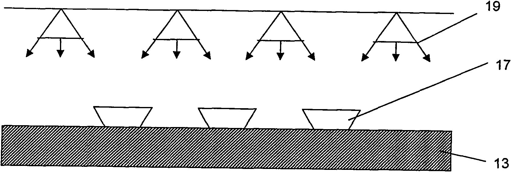
[0051] 2. Exposure: Adopt the contact exposure method, tile the surface of the photosensitive layer 14 with the mask plate 15 with the electrode pattern, then irradiate the mask plate 15 and the photosensitive layer 14 with ultraviolet light 16, the above-mentioned pattern mask in the exposure process The light diffraction and refraction of the plate 15 form a reverse trapezoid, and the ultraviolet light 16 penetrates the transparent area on the mask plate 15 and irradiates the corresponding position of the photosensitive layer 14, so that this part of the photosensitive material is cured to form a cured photosensitive material 17; The opaque area on the film plate 15 can block the irradiation of the ultraviolet light 16 and keep ...
example 2
[0057] In the above-mentioned example 1, the glass substrate with the electrode pattern is sintered under the firing conditions of 550°C and 15 minutes of heat preservation, which constitutes the second group of embodiments of the present invention.
PUM
| Property | Measurement | Unit |
|---|---|---|
| thickness | aaaaa | aaaaa |
| thickness | aaaaa | aaaaa |
| thickness | aaaaa | aaaaa |
Abstract
Description
Claims
Application Information
 - R&D Engineer
- R&D Manager
- IP Professional
- Industry Leading Data Capabilities
- Powerful AI technology
- Patent DNA Extraction
Browse by: Latest US Patents, China's latest patents, Technical Efficacy Thesaurus, Application Domain, Technology Topic.
© 2024 PatSnap. All rights reserved.Legal|Privacy policy|Modern Slavery Act Transparency Statement|Sitemap