Beam shaping illumination system of semiconductor laser array

A laser array and beam shaping technology, applied in semiconductor laser devices, semiconductor devices of light-emitting elements, laser devices, etc., can solve the problems of difficult integration, high production cost, low efficiency, etc.

Inactive Publication Date: 2009-09-30
ZHEJIANG UNIV
View PDF0 Cites 21 Cited by
  • Summary
  • Abstract
  • Description
  • Claims
  • Application Information

AI Technical Summary

Problems solved by technology

[0005] In order to overcome the shortcomings of the existing semiconductor laser array beam shaping lighting system, such as low efficiency, complex structure, difficult integration, and high production cost, the purpose of the present invention is to provide a semiconductor l

Method used


Image

  • Beam shaping illumination system of semiconductor laser array
  • Beam shaping illumination system of semiconductor laser array
  • Beam shaping illumination system of semiconductor laser array

Examples


Embodiment 1

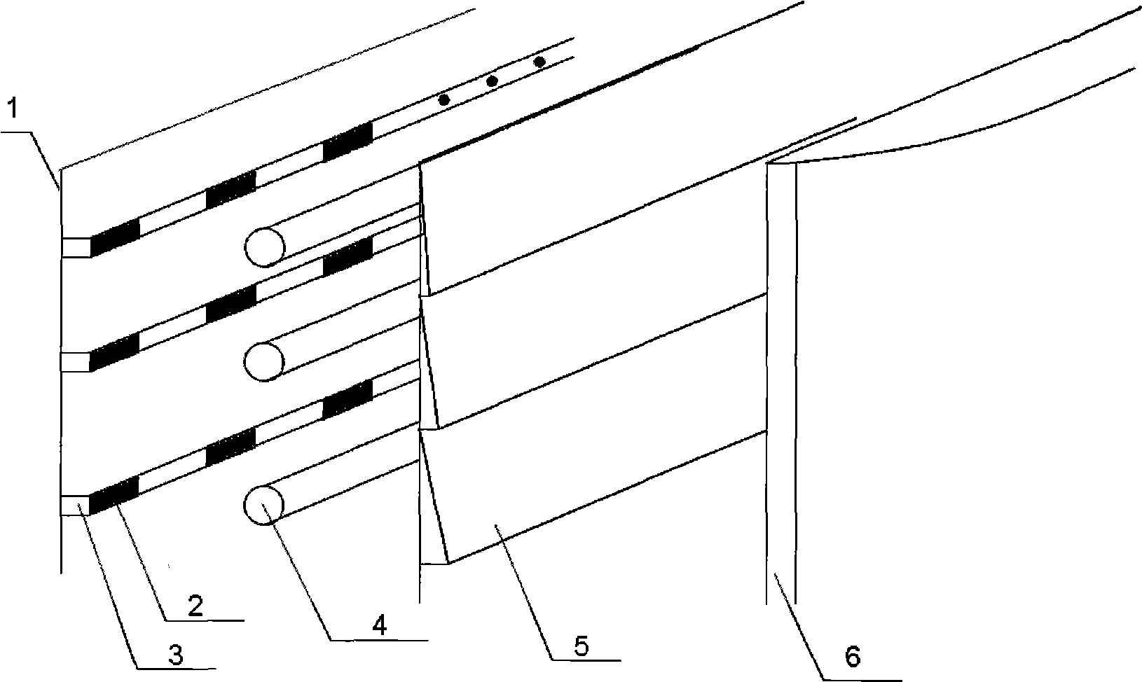
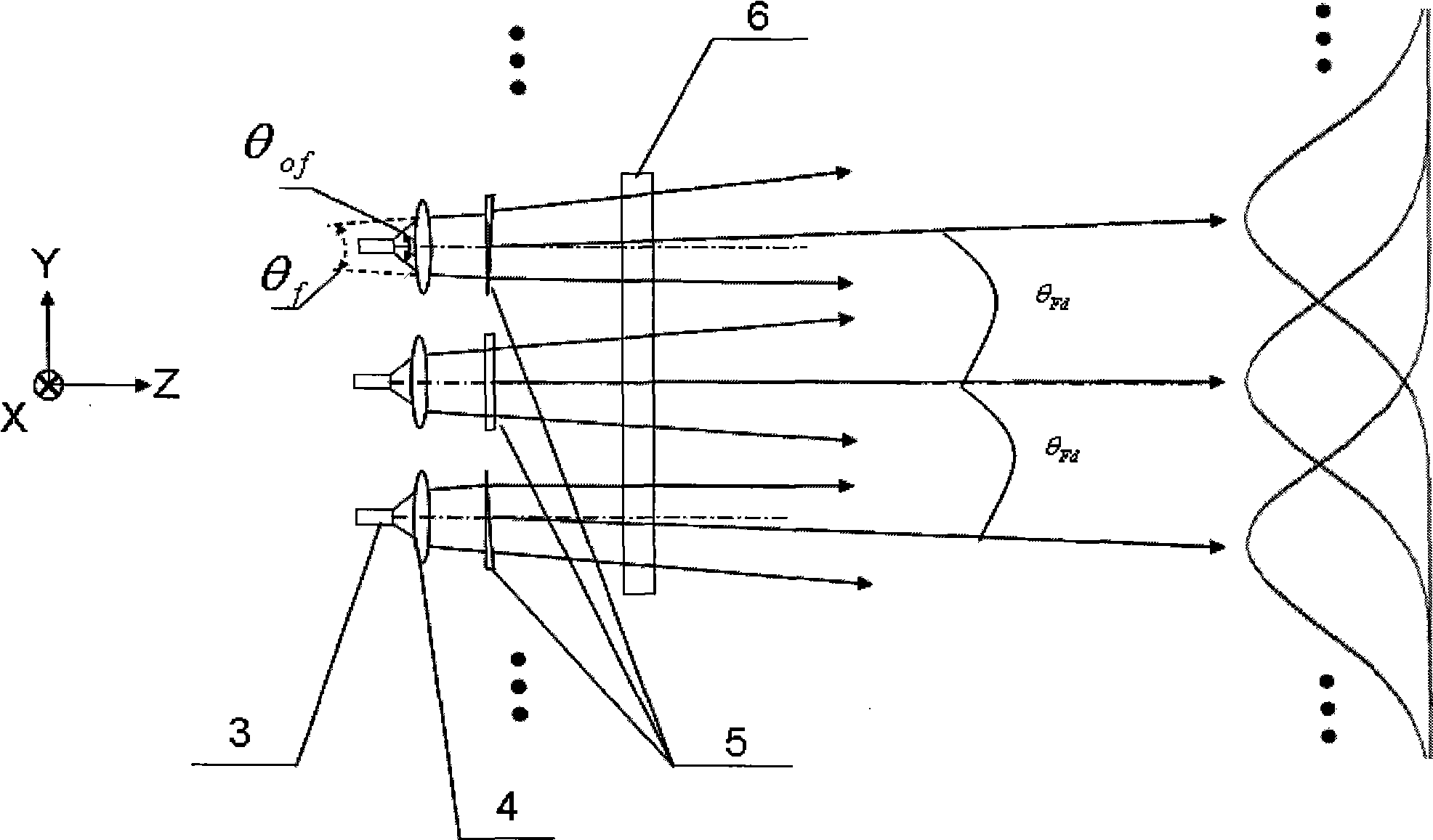
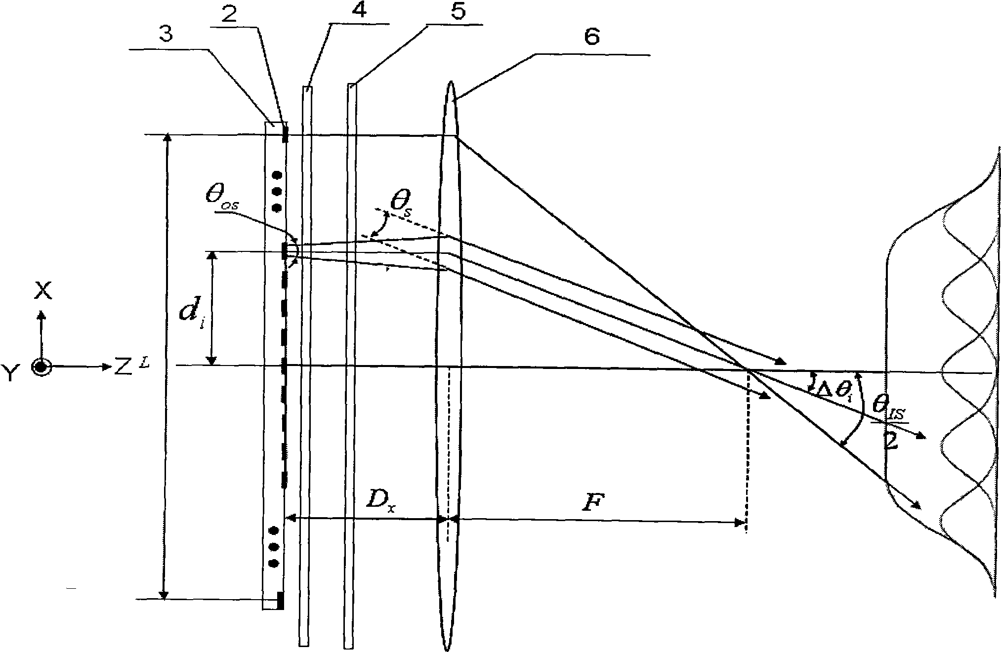
[0059] exist figure 1 Among them, the semiconductor laser two-dimensional array 1, the microcylindrical lens array 4, the optical wedge array 5, and the cylindrical lens 6 are arranged in sequence along the laser propagation direction, wherein each microcylindrical lens busbar of the microcylindrical lens array 4 is connected to the semiconductor laser The line direction of the line array 3 is parallel and arranged in one-to-one alignment, the unit optical wedges in the wedge array 5 are aligned and arranged in a one-to-one alignment with the semiconductor laser line array 3, and the busbar of the cylindrical lens 6 is perpendicular to the semiconductor laser line array 3 and The optical axis of the cylindrical lens 6 coincides with the mid-perpendicular line of the semiconductor laser bar array 3 . Take a 900W 808nm semiconductor laser stack array (stack) to form a 10-degree x 10-degree lighting system as an example. The semiconductor laser two-dimensional array 1 is a 900W 8...

Embodiment 2

[0061] exist figure 1 For the two-dimensional array of semiconductor lasers 1, the semiconductor laser unit 2, the semiconductor laser line array 3, the microcylindrical lens array 5, and the optical wedge array 6 Figure 5 , Figure 6 The semiconductor laser line array 7 and the geometrical surface base 8 with fast-axis divergence compressed micro-cylindrical lenses shown in . Take the 800W 808nm semiconductor laser stack array (stack) to form a 10-degree x 10-degree lighting system as an example, wherein the geometric surface base 8 can be as follows Figure 5 As shown, a convex cylindrical surface or a concave cylindrical surface equal to the fast axis field of view angle of 10 degrees, the semiconductor laser line array 7 with the fast axis divergence angle compressed microcylindrical lens is placed on the convex cylindrical surface or the concave cylindrical surface at equal intervals on, it can also be as Figure 6 The angle between the normals of two adjacent planes ...

Embodiment 3

[0063] Such as Figure 7 As shown, it is an integrated extension of the original system. A plurality of integral lighting system units 9 with the same lighting field of view angle are integrated and used as an array of units to increase the total power of the far-field lighting system and enhance uniformity.


PUM


Abstract

The invention discloses a beam shaping illumination system of a semiconductor laser array, which comprises the semiconductor laser array, an optical system for transforming beam divergence angles of a fast axis, a device for deflecting angles of beams in the fast axis direction, and an optical system for transforming divergence angles of a slow axis and deflecting the beams in the slow axis direction. The system has a key point that the superposition effect of Gaussian beam parts of a plurality of laser units is formed in a distant field by controlling the deflection degree of beam transmission axes of each laser unit in the fast axis and slow axis directions respectively so as to construct illumination beams according with field coverage requirements. The system has the characteristics of high efficiency, simple structure, low cost, integration and practicability, and is particularly applicable as an illumination light source of area array imaging laser radar and active laser illumination detecting systems.

Description

technical field [0001] The invention relates to a light beam shaping illumination system of a semiconductor laser array. Background technique [0002] In order to obtain integrated high-power output, the semiconductor laser array uses a semiconductor laser output module composed of semiconductor laser units in a series-parallel form. It has the characteristics of high output power, high photoelectric conversion efficiency, convenient laser intensity modulation, small size, and long life. It is very suitable for As an active illumination source for area array imaging lidar and laser detection systems. [0003] Semiconductor lasers have a special resonator structure and working mode, which makes the spatial distribution of the beam asymmetrical, with a divergence angle of about 40 degrees in the direction perpendicular to the junction plane (fast axis direction), and a divergence angle of about 40 degrees in the direction parallel to the junction plane. The upper (slow axis d...

Claims


Application Information

Patent Timeline
IPC IPC(8): F21K7/00H01S5/40F21V5/00G02B27/09F21K99/00F21K9/20F21Y115/30
Inventor 严惠民姜燕冰张秀达
Owner ZHEJIANG UNIV
Why Eureka
Try Eureka