Chip lug structure and manufacturing method thereof

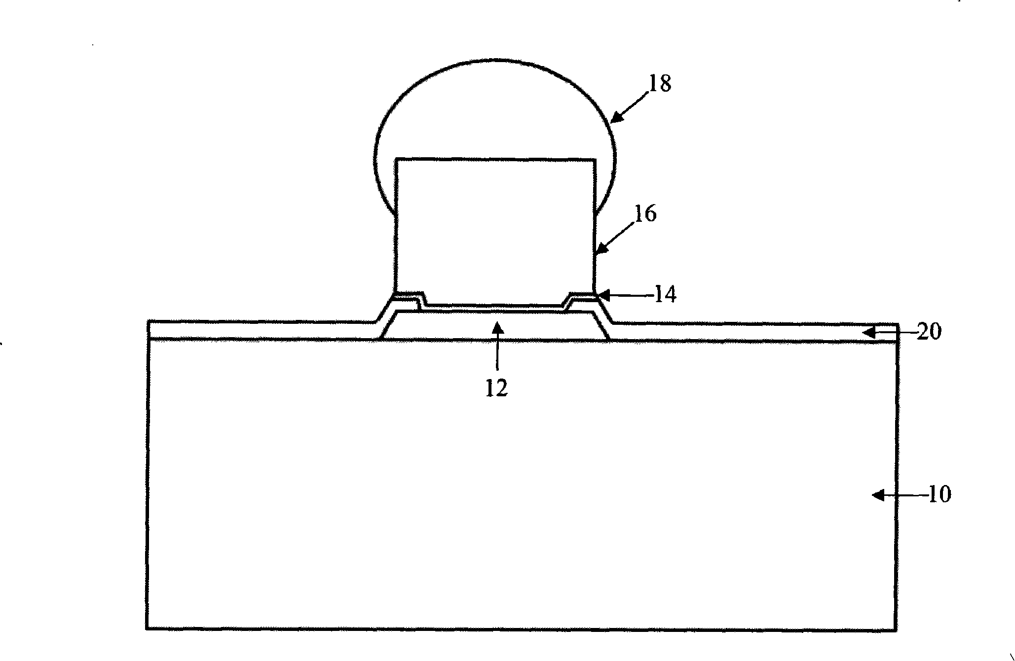
A manufacturing method and technology of bumps, which are applied in semiconductor/solid-state device manufacturing, electrical components, electric solid-state devices, etc., can solve problems such as difficulty in controlling the amount of solder in solder bumps 18, affecting packaging reliability, and unsatisfactory solder amount.

Inactive Publication Date: 2011-06-01
SEMICON MFG INT (SHANGHAI) CORP
View PDF0 Cites 0 Cited by
  • Summary
  • Abstract
  • Description
  • Claims
  • Application Information

AI Technical Summary

Problems solved by technology

Generally, different products have different requirements for the solder dose of the solder bump 18; however, in actual operation, the solder dose of the solder bump 18 is difficult to control
Because when the solder is reflowed to melt into a spherical shape, too much solder will flow down from the edge of the copper pillar 16, which will cause the amount of solder to not meet the requirements and affect the reliability of the package.

Method used


Image

  • Chip lug structure and manufacturing method thereof
  • Chip lug structure and manufacturing method thereof
  • Chip lug structure and manufacturing method thereof

Examples


Embodiment Construction

[0021] The present invention will be further described below in conjunction with the drawings and embodiments.

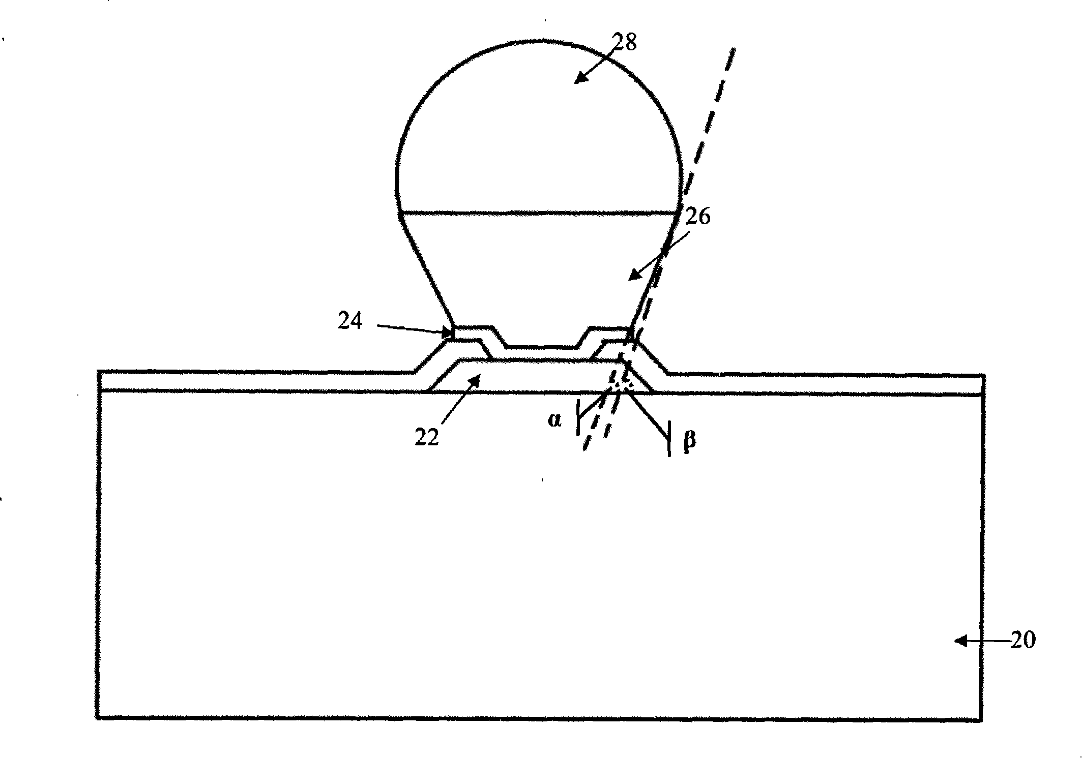
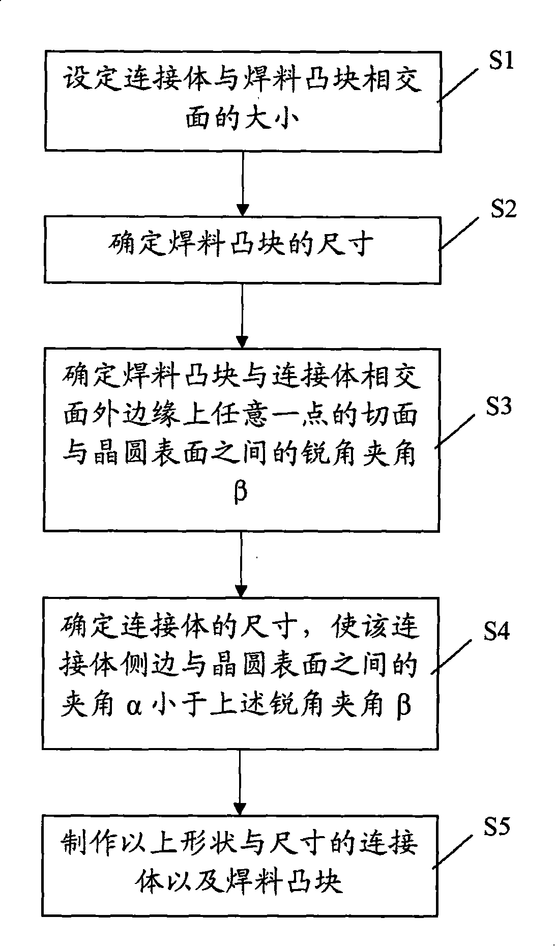
[0022] Please refer to figure 2 , Which is a schematic cross-sectional view of a chip bump structure provided by an embodiment of the present invention. As shown in the figure, the chip bump structure is formed on the solder pad 22 on the surface of the wafer 20, which includes a connecting body 26 on the solder pad and a solder bump 28 on the connecting body 26. The shape of the connecting body 26 For the table body. Generally, a first included angle α is formed between the side edge of the connecting body 26 and the surface of the wafer 20; the shape of the solder bump 28 is a partial sphere, and a cut surface at any point on the outer edge of the intersecting surface of the connecting body 26 and the wafer 20 A second included angle β smaller than 90 degrees is formed between the surfaces, wherein the first included angle α is smaller than the second included angl...


PUM


Abstract

The invention provides a chip lug structure and a manufacturing method thereof. A connector for the chip lug is designed into a table shape, and the inclination angle of the side of the connector is set according to the dosage of a solder for soldering the lug so as to meet the customization requirements of clients; and compared with the prior columnar connector, under the same section diameter, the connector of the invention can support the solder of more dosage and avoid the problem that the solder flows down from the edge of a copper column in a refluxing process. The chip lug structure ispositioned on a solder pad on the surface of a wafer, and comprises the connector positioned on the solder pad and a solder lug positioned on the connector, wherein the connector has the table shape.

Description

Technical field [0001] The invention relates to a semiconductor packaging structure and a manufacturing method thereof, in particular to a structure of a chip bump and a manufacturing method thereof. Background technique [0002] With the rapid development of semiconductor process technology, the functions of semiconductor chips are becoming more and more powerful, and the number of their pins has also increased. In order to meet the needs of the market, chip packaging technology is low-level dual in-line packaging (DIP) technology, etc. Gradually developed to high-end packaging technologies such as chip scale packaging (CSP). [0003] Among them, the chip-scale package is directly connected to the circuit board by bumping or ball mount, because there is no need for interposer, underfill and lead frame, and omitting die bonding, wire bonding, etc. The manufacturing process has greatly reduced material and labor costs, and has achieved rapid development. In the development process...

Claims


Application Information

Patent Timeline
Patent Type & Authority Patents(China)
IPC IPC(8): H01L23/485H01L21/60
CPCH01L24/11H01L2224/11H01L2924/00012
Inventor 李德君
Owner SEMICON MFG INT (SHANGHAI) CORP
Why Eureka
Try Eureka