Semiconductor module and inverter apparatus

A technology for semiconductors and substrates, which is applied in the field of having a base plate, and can solve the problems of reduced cooling performance and undisclosed composition.

Inactive Publication Date: 2010-01-06
AISIN AW CO LTD
View PDF1 Cites 3 Cited by
  • Summary
  • Abstract
  • Description
  • Claims
  • Application Information

AI Technical Summary

Problems solved by technology

Therefore, there is a problem that the temperature of the coolant flowing through each coolant channel 105 gradually rises, and the cooling performance of the switching element 106 on the downstream side decreases.
[0006] In addition, the aforementioned Patent Document 1 only discloses a configuration in which the switching elements 106 and the diode elements 107 of the substrates 104 are alternately arranged in a direction perpendicular to the flow direction D of the coolant.
There is

Method used


Image

  • Semiconductor module and inverter apparatus
  • Semiconductor module and inverter apparatus
  • Semiconductor module and inverter apparatus

Examples


no. 1 approach

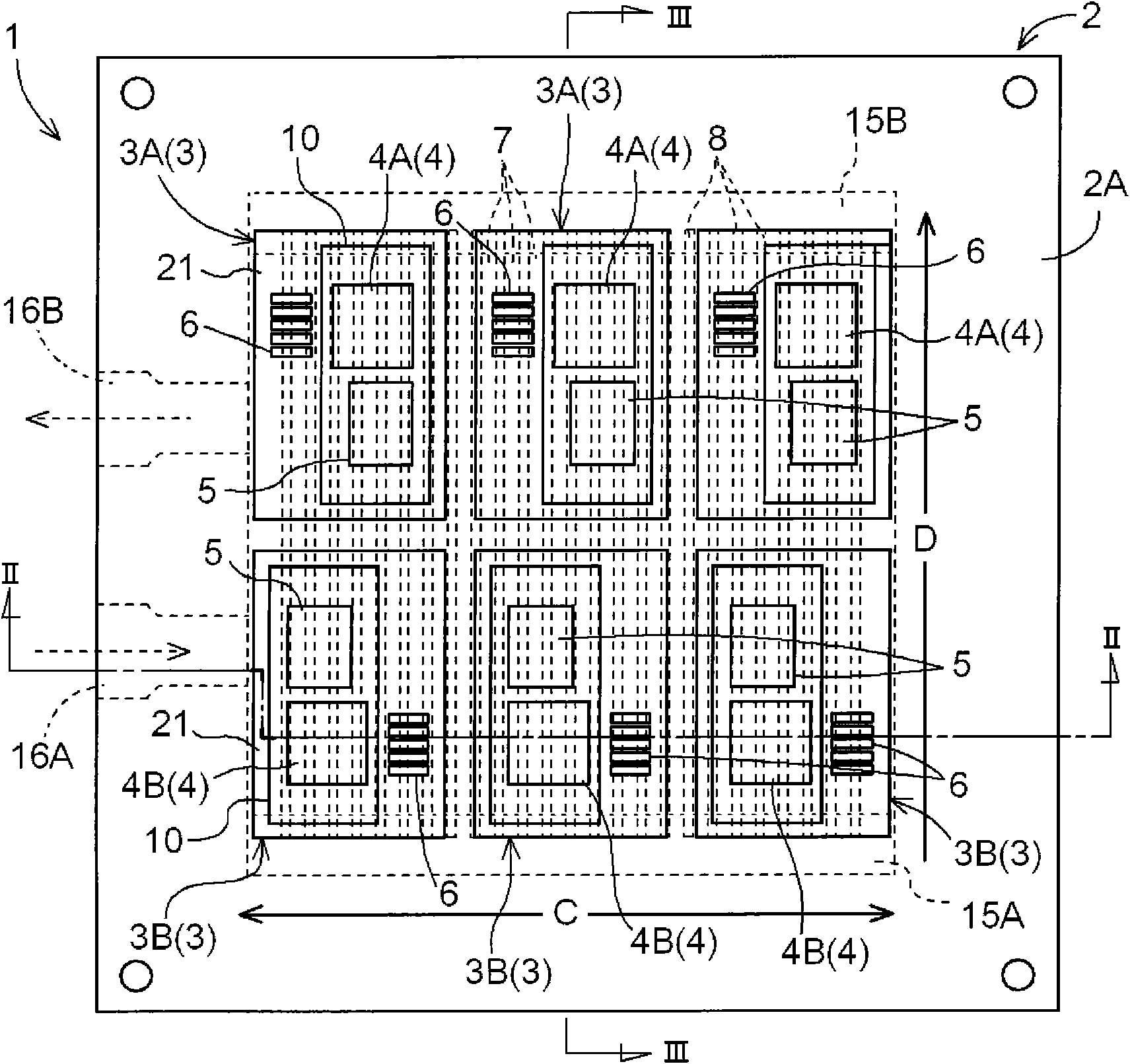
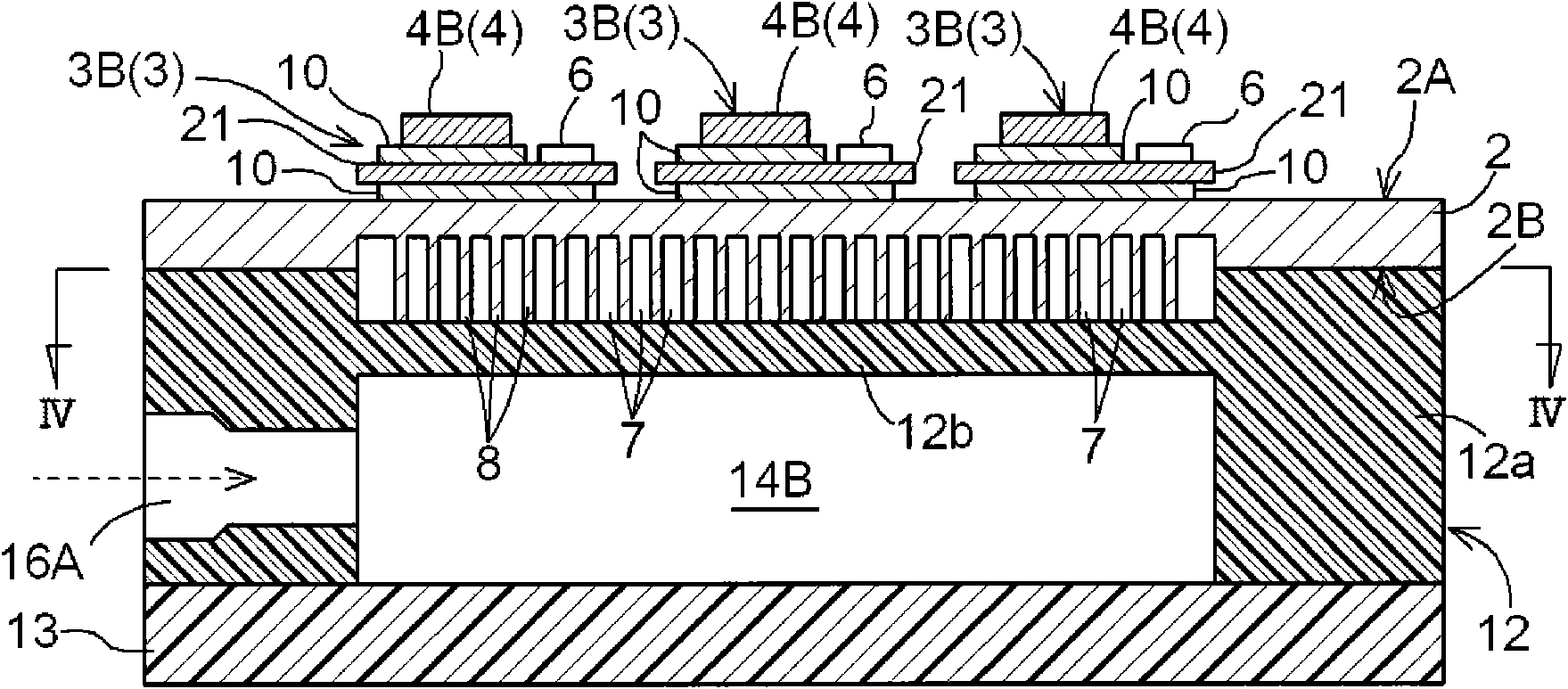
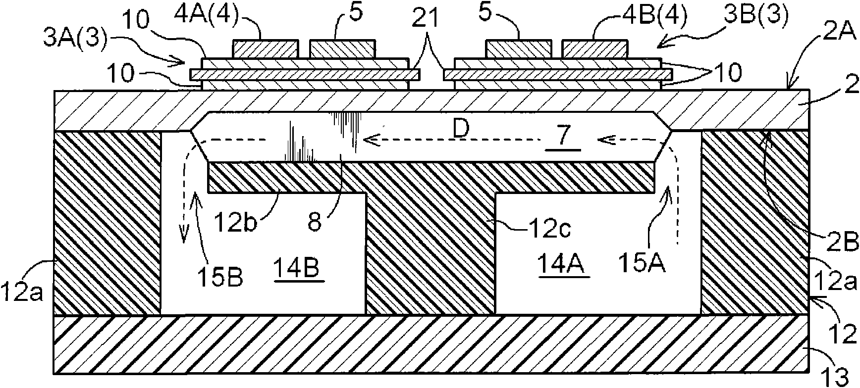
[0041] A first embodiment of the present invention will be described with reference to the drawings. In this embodiment, an example in which the present invention is applied to the semiconductor module 1 as an inverter device constituting a three-phase AC inverter circuit will be described. Figure 1 to Figure 8 It is a figure for demonstrating the structure of the semiconductor module 1 of this embodiment. Also, in Figure 1 to Figure 5 In , configurations other than the substrate 3 above the bottom plate 2 are omitted.

[0042] As shown in these figures, this semiconductor module 1 has a cooling structure including a coolant flow path 7 for cooling the switching element 4 of the substrate 3 placed on the upper surface 2A of the base plate 2, especially the most heat-generating. Allow to cool. Additionally, if Image 6 As shown, this semiconductor module 1 constitutes an inverter circuit 11 for driving a three-phase AC motor 31 . Therefore, if figure 1 As shown, six su...

no. 2 approach

[0070] A second embodiment of the present invention will be described with reference to the drawings. Figure 9 It is a plan view showing the configuration of the main part of the semiconductor module 1 of the present embodiment. As shown in this figure, the semiconductor module 1 of this embodiment is configured such that only one set consisting of a pair of lower arm substrate 3A and upper arm substrate 3B is placed on one base plate 2 . That is, the semiconductor module 1 of this embodiment differs from the above-mentioned first embodiment in the number of substrates 3 mounted on one base plate 2 . In addition, the point which is not specifically demonstrated in this embodiment can be the same as the structure of the said 1st embodiment.

[0071] Therefore, in the semiconductor module 1 of this embodiment, compared with the semiconductor module 1 of the first embodiment, the width in the vertical direction C of the base plate 2 is narrowed, and the overall width W of the c...

no. 3 approach

[0073] A third embodiment of the present invention will be described with reference to the drawings. Figure 10 It is a plan view showing the configuration of the main part of the semiconductor module 1 of the present embodiment. The semiconductor module 1 of this embodiment differs from the above-mentioned first and second embodiments in terms of the arrangement and configuration of the substrate 3 . Here, for the sake of simplification of drawings and the like, as in the above-mentioned second embodiment, only one set of a pair of substrates 3A, 3B is placed on one base plate 2 for description. In the same manner, it is also applicable to a configuration in which a pair of substrates 3A, 3B is used as a set and a plurality of sets of substrates 3 are placed on the bottom plate 2 . In addition, regarding the points not particularly described in this embodiment, the same configuration as that of the above-mentioned first embodiment or second embodiment can be employed.

[00...


PUM


Abstract

Provided is a semiconductor module having a structure in which a plurality of substrates each having a switching element and a diode element thereon are arranged such that the switching element and the diode element are disposed in series in the direction in which a refrigerant flows so that the switching elements on the respective substrates can be appropriately cooled. Parallel flow generating means (8) for generating parallel flows of the refrigerant in a predetermined direction are arranged in refrigerant flow paths (7). Each substrate (3) has thereon the switching element (4) and the diode element (5) such that those elements are disposed in series in the direction (D) in which the refrigerant flows. On each substrate, the switching element (4) and a connection terminal area (6) are arranged in different positions in the direction (C) orthogonal to the refrigerant flowing direction (D). The substrates (3) of each pair are disposed in series in the refrigerant flowing direction (D). In one of the substrates (3) of each pair, the switching element (4) is arranged on one side in the orthogonal direction (C), and in the other substrate (3), the connection terminal area (6) is disposed on that same side in the orthogonal direction (C).

Description

technical field [0001] The present invention relates to a base plate; a plurality of substrates mounted on one side of the base plate and provided with switching elements, diode elements, and connection terminal regions; and a coolant flow path provided in contact with the other side of the base plate. Semiconductor modules and inverter devices. Background technique [0002] For example, in an inverter circuit for driving a high-power output motor used in a hybrid vehicle, an electric vehicle, etc., a semiconductor module provided with a switching element constituting the inverter circuit generates a large amount of heat. , is also required to be miniaturized. Therefore, as a cooling structure for semiconductor modules, a water cooling system is often used. As a configuration of such a water-cooled semiconductor module, for example, the one disclosed in the following Patent Document 1 Figure 15 composition shown. In this figure, (a) is a top view, (b) is a side view, and...

Claims


Application Information

Patent Timeline
IPC IPC(8): H01L25/07H01L23/473H01L25/18H02M7/48
CPCH01L25/16H01L23/473H02M7/003H01L2224/73265H01L2924/3011H01L25/072H01L2224/48227H01L2224/32225H01L24/73H01L2924/1305H01L2924/13055H01L2924/00012H01L2924/00
Inventor 青木一雄鹤冈纯司安井诚二
Owner AISIN AW CO LTD
Why Eureka
Try Eureka