Pixel array
A pixel array and pixel technology, which is applied in the field of pixel arrays, can solve the problems of complex signals, high power consumption, and high cost of data drive chips, so as to reduce the number of data drive chips, lower costs, and reduce the number of layouts. Effect
- Summary
- Abstract
- Description
- Claims
- Application Information
AI Technical Summary
Problems solved by technology
Method used
Image
Examples
no. 1 example
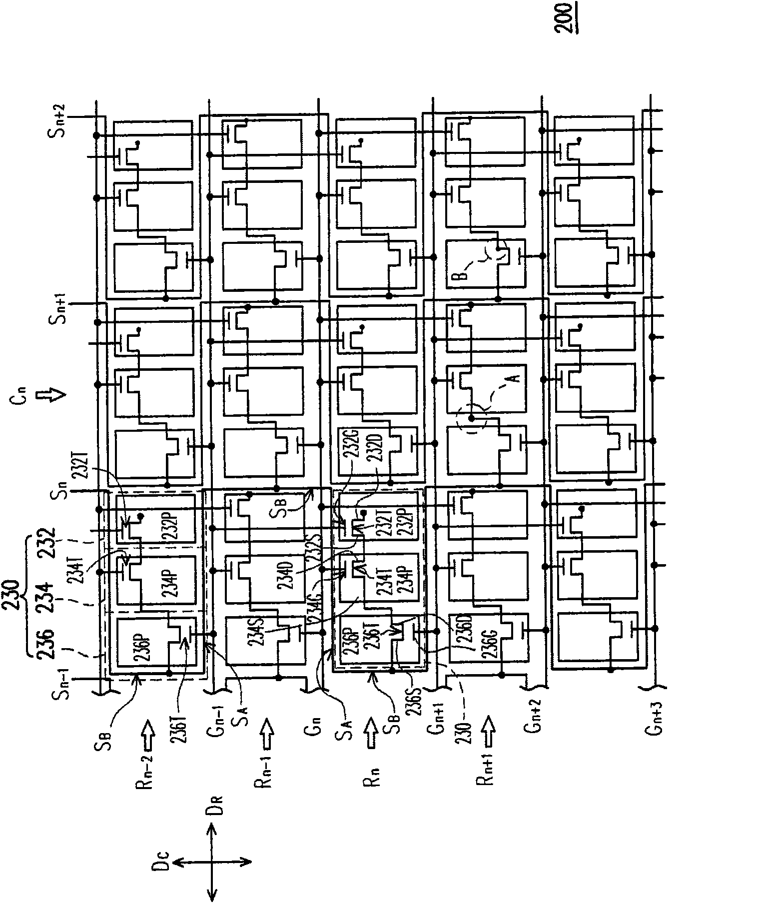
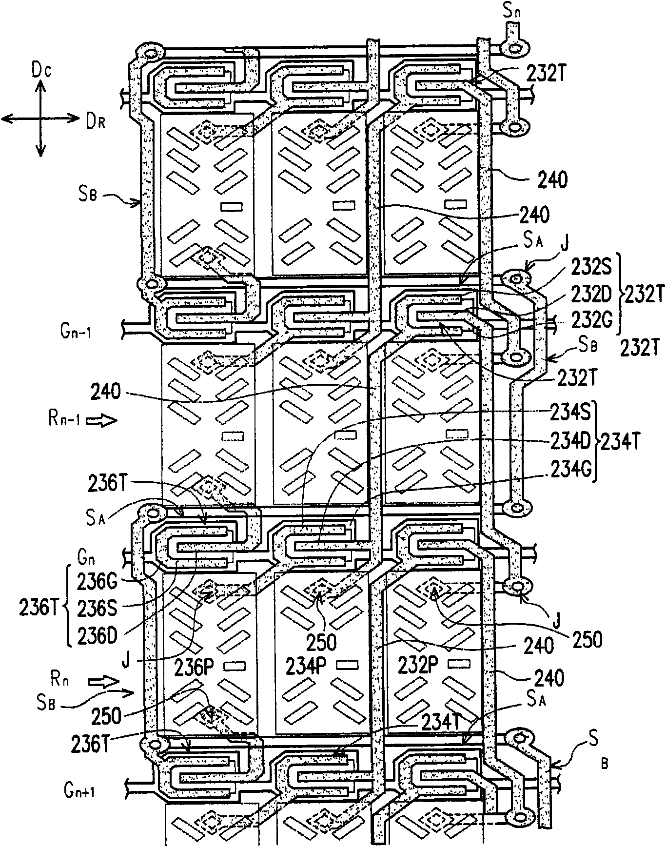
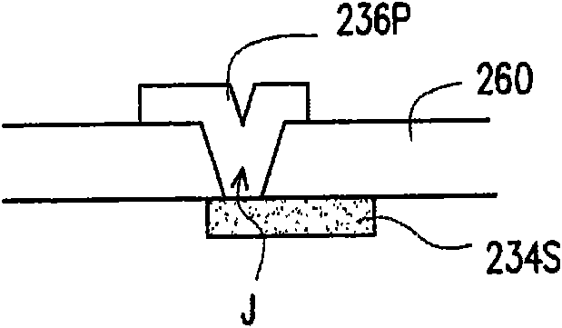
[0084] figure 1 It is a schematic layout diagram of a pixel array of the present invention. Please refer to figure 1 , the pixel array 200 includes a plurality of scan lines G, a plurality of data lines S and a plurality of pixels 230 , wherein the data lines S intersect the scan lines G. For clarity, let the pixel array 200 have a column direction D R and a row direction D C , and the column direction D R substantially orthogonal to the row direction D C . In this embodiment, a plurality of scanning lines G are generally along the column direction D R extended, while the multiple data lines S are generally along the row direction D C Zigzag extension. Such as figure 1 As shown, each pixel 230 in the pixel array 200 is connected to the corresponding scan line G and the corresponding data line S, especially, in this embodiment, the pixels 230 connected to the same data line S are only distributed in the said bar On the same side of the data line S, and arranged in the...
no. 2 example
[0107] Figure 4 It is a schematic layout diagram of a pixel array according to the second embodiment of the present invention. Please refer to Figure 4 , the pixel array 300 of this embodiment is similar to that of the first embodiment, so similar components are denoted by the same reference numerals as those of the first embodiment. However, compared with the first embodiment, in the pixel array 300 of this embodiment, the winding design of the data line S is changed to a straight line design, and the scanning line G is further designed as a winding design.
[0108] In detail, in this embodiment, arranged in the nth column R n In each pixel 230, the first transistor 232T, the first pixel electrode 232P, the second transistor 234T, the second pixel electrode 234P, the third transistor 236T and the third pixel electrode 236P are all located on the nth scanning line G n with the n+1th scan line G n+1 between. and if Figure 4 As shown, each scan line G is substantially i...
no. 3 example
[0117] Figure 6 It is a schematic layout diagram of a pixel array according to the third embodiment of the present invention. Please refer to Figure 6, the pixel array 400 of this embodiment is similar to that of the second embodiment, so similar components are denoted by the same reference numerals as those of the previous embodiment. However, compared with the foregoing embodiments, in the pixel array 400 of this embodiment, the design of the transistors is different from that of the second embodiment.
[0118] In detail, such as Figure 6 as shown, Figure 6 with the aforementioned second embodiment Figure 4 Similarly, arranged in the nth column R n In each pixel 230, the first transistor 232T, the first pixel electrode 232P, the second transistor 234T, the second pixel electrode 234P, the third transistor 236T and the third pixel electrode 236P are also located on the nth scanning line G n with the n+1th scan line G n+1 between. And, each fourth wire G B The le...
PUM
 Abstract
Description
Claims
Application Information
 - R&D
- Intellectual Property
- Life Sciences
- Materials
- Tech Scout
- Unparalleled Data Quality
- Higher Quality Content
- 60% Fewer Hallucinations
Browse by: Latest US Patents, China's latest patents, Technical Efficacy Thesaurus, Application Domain, Technology Topic, Popular Technical Reports.
© 2025 PatSnap. All rights reserved.Legal|Privacy policy|Modern Slavery Act Transparency Statement|Sitemap|About US| Contact US: help@patsnap.com


