Display and method for driving the display

A technology of display device and display area, which is applied to lighting devices, static indicators, input/output process of data processing, etc., can solve the problems of display device thickness, weight increase, display quality damage, etc., to prevent display characteristics Deterioration and the effect of reducing the fluctuation of capacitance

Active Publication Date: 2010-01-20
NEC LCD TECH CORP
View PDF10 Cites 20 Cited by
  • Summary
  • Abstract
  • Description
  • Claims
  • Application Information

AI Technical Summary

Problems solved by technology

However, in the above case, there are the following problems: the thickness and weight of the display device are increased due to the thickness of the contact sensor itself; the display quality is impaired due to the parts covering the screen

Method used


Image

  • Display and method for driving the display
  • Display and method for driving the display
  • Display and method for driving the display

Examples


no. 1 Embodiment approach

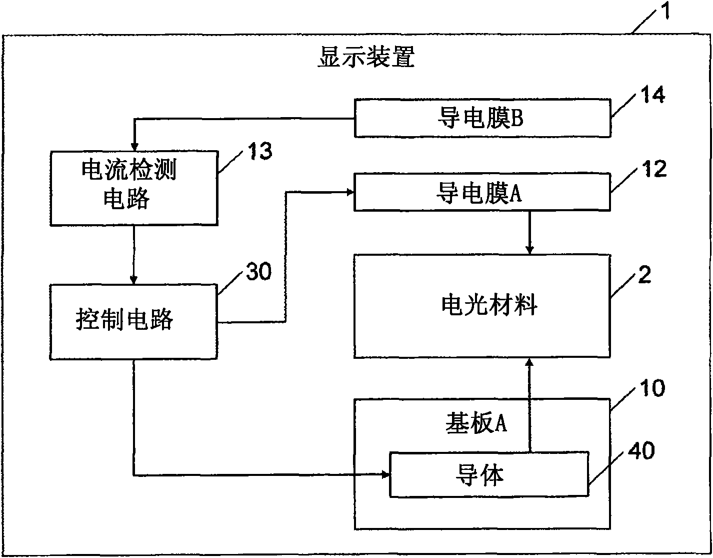
[0067] figure 1 It is a block diagram showing the configuration of the display device according to the first embodiment of the present invention. refer to figure 1 , the display device 1 has an electro-optic material 2 , a conductor 40 , a conductive film A 12 , a conductive film B 14 , a current detection circuit 13 , and a control circuit 30 .

[0068] The conductor 40 provides an electrical signal to the electro-optical material 2 . The conductive film A 12 supplies electrical signals to the electro-optical material 2 . The conductive film B 14 is provided on the display surface of the display device 1 . The current detection circuit 13 detects the current in the conductive film B 14 . During the period when the current detection circuit 13 detects the current, the control circuit 30 applies a voltage approximately the same as that of the conductive film B14 to any one of the conductor 40 and the conductive film A12, and makes the other floating (Floating), or applies...

no. 2 Embodiment approach

[0073] A display device according to a second embodiment of the present invention will be described with reference to the drawings.

[0074] (composition description)

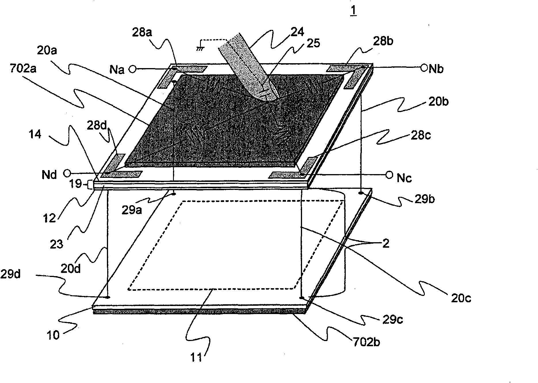
[0075] figure 2 It is a perspective view of the display device according to the second embodiment of the present invention. The display device 1 has a substrate A 10 , an opposing substrate 19 , an electro-optical material (such as liquid crystal) 2 sandwiched between these substrates, and polarizing plates 702 a and 702 b.

[0076] The opposite substrate 19 includes: a substrate B (glass substrate, etc.) 23; a color filter (not shown), formed on the surface of the liquid crystal side of the substrate B 23; a conductive film A 12, formed on the liquid crystal of the color filter A surface on one side; a conductive film B14 is formed on the surface on the opposite side of the substrate B23. The conductive film A12 and the conductive film B14 may be a transparent conductive film formed of ITO as an example. ...

no. 3 Embodiment approach

[0148] A third embodiment of the present invention will be described with reference to the drawings. Figure 16 It is a perspective view of an example of a display device according to this embodiment. This embodiment is a modification of the second embodiment described above. In the second embodiment, the counter substrate 19 and the conductive film B14 are integrally formed. In this embodiment, however, the protective substrate 705 and the conductive film B (position detection conductive film) 14 are integrally formed. The structure of the substrate A (display device substrate) 10 is the same as that in the second embodiment.

[0149] The opposite substrate 19 has: a substrate B 23; a color filter (not shown), formed on the surface of the electro-optic material 2 side of the substrate B 23; a conductive film A 12, formed on the electro-optic material 2 of the color filter- side face. The conductive film A 12 and the substrate A 10 are electrically connected through the co...


PUM

PropertyMeasurementUnit
capacitanceaaaaaaaaaa

Abstract

A display comprising: an electro-optical material arranged between first and second planes facing each other; a first substrate arranged on the first plane and including a conductor that affords an electrical signal to the electro-optical material; a first electrically conductive film arranged on the second plane to afford an electrical signal to the electro-optical material; a second electrically conductive film arranged outside an area sandwiched between the first and second planes; and a current detection circuit that detects the current on the second electrically conductive film. The display further comprises a control circuit that, during a time period the current is detected by the current detection circuit, applies substantially the same voltage as that applied to the second electrically conductive film to one of the conductor and the first electrically conductive film, which is arranged more proximate to the second electrically conductive film, and sets the other in a floating state, or applies substantially the same voltage as that applied to the second electrically conductive film to both the conductor and the first electrically conductive film.

Description

technical field [0001] The present invention relates to a display device and a driving method of the display device, in particular to a display device and a driving method of the display device for detecting position coordinates indicated by a finger or a pen on a display surface or detecting whether there is an indication action. Background technique [0002] The contact sensor is a device that detects the position coordinates indicated by fingers, pens, etc. or whether there is an indicated action. It is usually used in combination with display devices such as Liquid Crystal Display (LCD) and Plasma Display Panel (PDP). . [0003] By inputting the output of the touch sensor to the computer, the display content of the display device is controlled by the computer, or the equipment is controlled, so that a man-machine interface with good operability can be realized. Today, contact sensors are widely used in daily life such as game machines, mobile information terminals, tick...

Claims


Application Information

Patent Timeline
Patent Type & Authority Applications(China)
IPC IPC(8): G02F1/133G02F1/167G02F1/15H05B33/14G09G3/20G09G3/36G06F3/041
CPCG06F3/0412G06F3/0443G06F3/042
Inventor 芳贺浩史柳濑慈郎北岸洋一
Owner NEC LCD TECH CORP
Why Eureka
Try Eureka