Solar cell and manufacturing method thereof

A solar cell and back electrode technology, applied in circuits, photovoltaic power generation, electrical components, etc., can solve the problems of complex manufacturing process, reduced light efficiency, increased defects, etc., and achieve the effect of maximizing light absorption and increasing reflection coefficient

Inactive Publication Date: 2010-01-20
SAMSUNG ELECTRONICS CO LTD +1
View PDF3 Cites 5 Cited by
  • Summary
  • Abstract
  • Description
  • Claims
  • Application Information

AI Technical Summary

Problems solved by technology

[0007] However, the manufacturing process for the textured transparent conductive layer between the back electrode layer and the light absorbing layer is complicated, and the light efficiency will be lowered by the transparent conductive layer, which has lower conductivity than the metal of the back electrode layer. Conductivity
Also, since the contact interface between layers increases, the probability of defect generation increases

Method used


Image

  • Solar cell and manufacturing method thereof
  • Solar cell and manufacturing method thereof
  • Solar cell and manufacturing method thereof

Examples


Embodiment Construction

[0038] Exemplary embodiments of the present invention will be described in more detail below with reference to the accompanying drawings. As those skilled in the art would realize, the described embodiments may be modified in various ways, all without departing from the spirit or scope of the present invention. The exemplary embodiments of the present invention provide those skilled in the art with a complete disclosure of the nature and scope of the present invention.

[0039] In the drawings, the thickness of layers, films, panels, regions, etc., are exaggerated for clarity. Like reference numerals refer to like elements throughout the specification. It will be understood that when an element such as a layer, film, region, or substrate is referred to as being "on" another element, it can be directly on the other element or intervening elements may also be present.

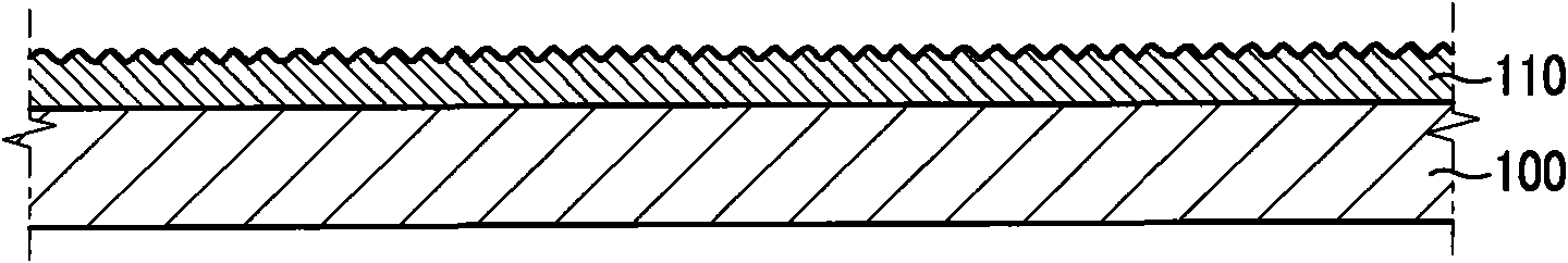
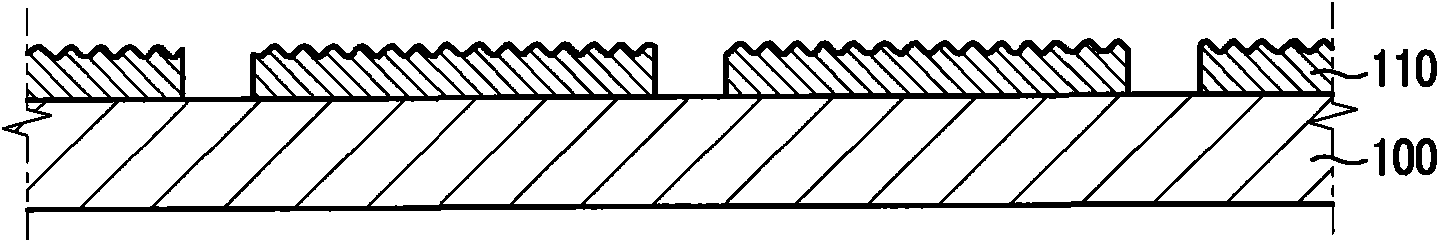
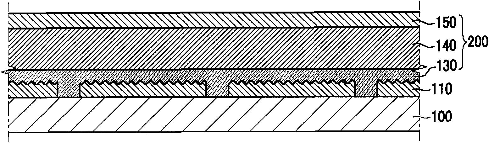
[0040] Figure 1 to Figure 7 are cross-sectional views sequentially illustrating manufacturing processes in ...


PUM

PropertyMeasurementUnit
sizeaaaaaaaaaa
sizeaaaaaaaaaa

Abstract

A method for manufacturing a solar cell is provided. The manufacturing method includes: depositing a transparent conductive layer on a substrate; patterning the transparent conductive layer; forming a semiconductor layer including deposited on the patterned transparent conductive layer; patterning the semiconductor layer; coating a metal powder on the patterned semiconductor layer; forming a rear electrode layer on the semiconductor layer coated with the metal powder; and patterning the rear electrode layer and the semiconductor layer. This method is useful for producing a solar cell with improved light absorption efficiency.

Description

technical field [0001] The invention relates to a solar cell and a manufacturing method thereof. Background technique [0002] A solar cell that converts sunlight energy into electricity generates electricity by using two types of semiconductors called P-type semiconductors and N-type semiconductors. Solar cells can be mainly classified into crystalline silicon solar cells used in most commercial products, thin film solar cells that can use inexpensive substrates, and hybrid solar cells that combine crystalline silicon solar cells and thin film solar cells. [0003] In the present invention, a thin film solar cell is formed by coating a film on a thin glass or plastic substrate. Generally, the spread distance of carriers is shorter in thin-film solar cells than in crystalline silicon solar cells, and when the thin film is made of only a P-N junction structure, the collection efficiency of electron-hole pairs generated by sunlight very low. Therefore, a thin film utilizing...

Claims


Application Information

Patent Timeline
Patent Type & Authority Applications(China)
IPC IPC(8): H01L31/18H01L31/042H01L31/075H01L31/0232
CPCH01L31/0527Y02E10/52H01L31/076H01L31/022425Y02E10/548H01L27/1423Y02E10/50H01L31/046H01L31/0465H01L31/056H01L31/075H01L31/18H01L31/0445
Inventor 朴敏吴旼锡申明勋李昌昊李秉奎南毓铉郑胜在林美花徐晙荣
Owner SAMSUNG ELECTRONICS CO LTD
Why Eureka
Try Eureka